- 您現(xiàn)在的位置:買賣IC網(wǎng) > PDF目錄359784 > VND600TR-E (意法半導(dǎo)體) DOUBLE CHANNEL HIGH SIDE DRIVER PDF資料下載
參數(shù)資料
| 型號(hào): | VND600TR-E |
| 廠商: | 意法半導(dǎo)體 |
| 英文描述: | DOUBLE CHANNEL HIGH SIDE DRIVER |
| 中文描述: | 雙通道高邊驅(qū)動(dòng)器 |
| 文件頁(yè)數(shù): | 9/18頁(yè) |
| 文件大小: | 245K |
| 代理商: | VND600TR-E |
第1頁(yè)第2頁(yè)第3頁(yè)第4頁(yè)第5頁(yè)第6頁(yè)第7頁(yè)第8頁(yè)當(dāng)前第9頁(yè)第10頁(yè)第11頁(yè)第12頁(yè)第13頁(yè)第14頁(yè)第15頁(yè)第16頁(yè)第17頁(yè)第18頁(yè)
9/18
VND600-E
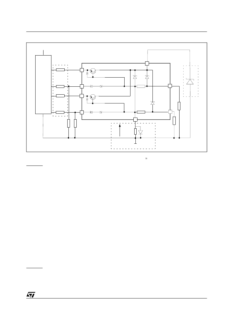
Figure 8. Application Schematic
GND
REVERSE BATTERY
Solution 1: Resistor in the ground line (R
GND
only). This
can be used with any type of load.
The following is an indication on how to dimension the
R
GND
resistor.
1) R
GND
≤
600mV / I
S(on)max
.
2) R
GND
≥ (
V
CC
) / (-I
GND
)
where -I
GND
is the DC reverse ground pin current and can
be found in the absolute maximum rating section of the
device’s datasheet.
Power Dissipation in R
GND
(when V
CC
<0: during reverse
battery situations) is:
P
D
= (-V
CC
)
2
/R
GND
This resistor can be shared amongst several different
HSD. Please note that the value of this resistor should be
calculated with formula (1) where I
becomes the
sum of the maximum on-state currents of the different
devices.
Please note that if the microprocessor ground is not
common with the device ground then the R
GND
will
produce a shift (I
S(on)max
* R
GND
) in the input thresholds
and the status output values. This shift will vary
depending on how many devices are ON in the case of
several high side drivers sharing the same R
GND
.
If the calculated power dissipation leads to a large
resistor or several devices have to share the same
resistor then the ST suggests to utilize Solution 2 (see
below).
Solution 2: A diode (D
GND
) in the ground line.
A resistor (R
GND
=1k
)
should be inserted in parallel to
D
GND
if the device will be driving an inductive load.
This small signal diode can be safely shared amongst
several different HSDs.
PROTECTION
NETWORK
AGAINST
Also in this case, the presence of the ground network will
produce a shift (
j
600mV) in the input thresholds and the
status output values if the microprocessor ground is not
common with the device ground. This shift will not vary if
more than one HSD shares the same diode/resistor
network.
Series resistor in INPUT and STATUS lines are also
required to prevent that, during battery voltage transient,
the current exceeds the Absolute Maximum Rating.
Safest configuration for unused INPUT and STATUS pin
is to leave them unconnected.
LOAD DUMP PROTECTION
D
is necessary (Voltage Transient Suppressor) if the
load dump peak voltage exceeds V
CC
max DC rating.
The same applies if the device will be subject to
transients on the V
CC
line that are greater than the ones
shown in the ISO T/R 7637/1 table.
.
μ
C I/Os PROTECTION:
If a ground protection network is used and negative
transient are present on the V
line, the control pins will
be pulled negative. ST suggests to insert a resistor (R
prot
)
in line to prevent the
μ
C I/Os pins to latch-up.
The value of these resistors is a compromise between
the leakage current of
μ
C and the current required by the
HSD I/Os (Input levels compatibility) with the latch-up lim-
it of
μ
C I/Os.
-V
CCpeak
/I
latchup
≤
R
prot
≤
(V
OH
μ
C
-V
IH
-V
GND
) / I
IHmax
Calculation example:
For V
CCpeak
= - 100V and I
latchup
≥
20mA; V
OH
μ
C
≥
4.5V
5k
≤
R
prot
≤
65k
.
Recommended R
prot
value is 10k
.
V
CC
GND
OUTPUT2
CURRENT SENSE1
D
ld
+5V
R
prot
R
SENSE2
OUTPUT1
R
SENSE1
INPUT1
D
GND
R
GND
V
GND
CURRENT SENSE2
INPUT2
μ
C
R
prot
R
prot
R
prot
相關(guān)PDF資料 |
PDF描述 |
|---|---|
| VNQ5050KTR-E | QUAD CHANNEL HIGH SIDE DRIVER FOR AUTOMOTIVE APPLICATIONS |
| VT5365V032 | Single-chip optical mouse sensor for wireless applications |
| VN750B5TR-E | HIGH SIDE DRIVER |
| VN750-E | HIGH SIDE DRIVER |
| VN750PT-E | HIGH SIDE DRIVER |
相關(guān)代理商/技術(shù)參數(shù) |
參數(shù)描述 |
|---|---|
| VND610SP | 制造商:未知廠家 制造商全稱:未知廠家 功能描述: |
| VND620SP | 制造商:STMicroelectronics 功能描述:HSD 40V 2X.03OHM - Rail/Tube |
| VND670SP | 功能描述:功率驅(qū)動(dòng)器IC Dual Hi-Side Switch RoHS:否 制造商:Micrel 產(chǎn)品:MOSFET Gate Drivers 類型:Low Cost High or Low Side MOSFET Driver 上升時(shí)間: 下降時(shí)間: 電源電壓-最大:30 V 電源電壓-最小:2.75 V 電源電流: 最大功率耗散: 最大工作溫度:+ 85 C 安裝風(fēng)格:SMD/SMT 封裝 / 箱體:SOIC-8 封裝:Tube |
| VND670SP_08 | 制造商:STMICROELECTRONICS 制造商全稱:STMicroelectronics 功能描述:Dual high-side switch with dual Power MOSFET gate driver(bridge configuration) |
| VND670SP13TR | 功能描述:功率驅(qū)動(dòng)器IC Dual Hi-Side Switch RoHS:否 制造商:Micrel 產(chǎn)品:MOSFET Gate Drivers 類型:Low Cost High or Low Side MOSFET Driver 上升時(shí)間: 下降時(shí)間: 電源電壓-最大:30 V 電源電壓-最小:2.75 V 電源電流: 最大功率耗散: 最大工作溫度:+ 85 C 安裝風(fēng)格:SMD/SMT 封裝 / 箱體:SOIC-8 封裝:Tube |
發(fā)布緊急采購(gòu),3分鐘左右您將得到回復(fù)。