- 您現(xiàn)在的位置:買(mǎi)賣(mài)IC網(wǎng) > PDF目錄359397 > VN050H (意法半導(dǎo)體) HIGH SIDE SMART POWER SOLID STATE RELAY PDF資料下載
參數(shù)資料
| 型號(hào): | VN050H |
| 廠商: | 意法半導(dǎo)體 |
| 英文描述: | HIGH SIDE SMART POWER SOLID STATE RELAY |
| 中文描述: | 高邊智能電源固態(tài)繼電器 |
| 文件頁(yè)數(shù): | 4/10頁(yè) |
| 文件大?。?/td> | 227K |
| 代理商: | VN050H |
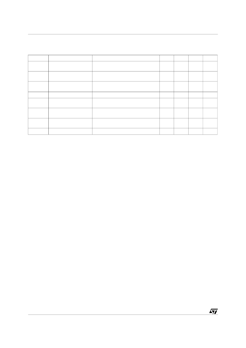
ELECTRICAL CHARACTERISTICS
(Continued)
PROTECTION AND DIAGNOSTICS
Symbol
V
STAT
(
)
Parameter
Test Conditions
Min.
Typ.
Max.
Unit
Status Voltage Output
Low
Under Voltage Shut
Down
Status Clamp Voltage
I
STAT
= 1.6 mA
0.4
v
V
USD
5.5
V
V
SCL
(
)
I
STAT
= 10 mA
I
STAT
= -10 mA
R
LOAD
< 10 m
R
LOAD
< 10 m
T
c
= 85
o
C
6
-0.7
V
V
I
OV
Over Current
20
A
I
AV
Average Current in
Short Circuit
Open Load Current
Level
Termal Shut-Down
Temperature
Reset Temperature
1.4
A
I
OL
5
180
mA
T
TSD
140
o
C
T
R
125
o
C
(*) The VIH is internally clamped at 6V about. it is possible to connect thispin to an higher voltage via an external resistor calculated to not
exceed 10 mA at the input pin.
(
) Status determinaion > 100
μ
s after the switching edge.
Note 1: Above V
CC
= 36V the output voltage is clamped to 36V. Power dissipation increases and the device turns off it junction temperature
reaches thermal shutdown temperature.
FUNCTIONAL DESCRIPTION
The device has a diagnostic output which
indicates open circuit (no load) and over
temperature conditions. The output signals are
processed by internal logic.
To protect the device against short circuit and
over-current condition the thermal protection
turns the integrated Power MOS off at a minimum
junction temperature of 140
temperature returns to about 125
o
C the switch is
automatically turned on again. To ensur the
protection in all V
CC
conditions and in all the
junction temperature range it is necessary to limit
the voltage drop across Drain and Source (pin 3
and 5) at 29 V. The device is able to withstand a
load dump according the test pulse 5 at level III of
the ISO TR/1 7631.
Above V
CC
= 36V the output voltage is clamped
to 36V. Power dissipation increases and the
device turns off if junction temperature reaches
thermal shutdown temperature.
o
C. When the
PROTECTING
REVERSE BATTERY
The simplest way to protect the device against a
continuous reverse battery voltage (-26V) is to
THE
DEVICE
AGAINST
insert a Schottky diode between pin 1 (GND) and
ground, as shown in the typical application circuit
(fig. 3).
The consequences of the voltage drop across
this diode are as follows:
-
If the input is pulled to power GND, a negative
voltage of -V
F
is seen by the device. (V
IL
, V
IH
thresholds and V
STAT
are increased by V
F
with
respect to power GND).
-
The undervoltage shutdown level is increased
by V
F
.
If there is no need for the control unit to handle
external analog signals referred to the power
GND, the best approach is to connect the
reference potential of the control unit to node [1]
(see application circuit infig. 4), which becomes
the common signal GND for the whole control
board.
In this way no shift of V
IH
, V
IL
and V
STAT
takes
place and no negative voltage appears on the
INPUT pin; this solution allows the use of a
standard diode, with a breakdown voltage able to
handle any ISO normalized negative pulses that
occours in the automotive environment.
VN05H
4/10
相關(guān)PDF資料 |
PDF描述 |
|---|---|
| VN050H(012Y) | Shielded Paired Cable; Number of Conductors:12; Conductor Size AWG:18; No. Strands x Strand Size:19 x 30; Jacket Material:Polyvinylchloride (PVC); Number of Pairs:6; Leaded Process Compatible:Yes; Features:Overall Beldfoil Shield RoHS Compliant: Yes |
| VN0540N3 | TRANSISTOR | MOSFET | N-CHANNEL | 400V V(BR)DSS | 100A I(D) | TO-92 |
| VN0540 | N-Channel Enhancement-Mode Vertical DMOS FETs |
| VN0545 | N-Channel Enhancement-Mode Vertical DMOS FETs |
| VN0550N3-G | N-Channel Enhancement-Mode Vertical DMOS FETs |
相關(guān)代理商/技術(shù)參數(shù) |
參數(shù)描述 |
|---|---|
| VN050H(011Y) | 制造商:STMICROELECTRONICS 制造商全稱(chēng):STMicroelectronics 功能描述:HIGH SIDE SMART POWER SOLID STATE RELAY |
| VN050H(012Y) | 制造商:STMICROELECTRONICS 制造商全稱(chēng):STMicroelectronics 功能描述:HIGH SIDE SMART POWER SOLID STATE RELAY |
| VN050H011Y | 制造商:STMICROELECTRONICS 制造商全稱(chēng):STMicroelectronics 功能描述:HIGH SIDE SMART POWER SOLID STATE RELAY |
| VN050H012Y | 制造商:STMICROELECTRONICS 制造商全稱(chēng):STMicroelectronics 功能描述:HIGH SIDE SMART POWER SOLID STATE RELAY |
| VN0540 | 制造商:SUPERTEX 制造商全稱(chēng):SUPERTEX 功能描述:N-Channel Enhancement-Mode Vertical DMOS FETs |
發(fā)布緊急采購(gòu),3分鐘左右您將得到回復(fù)。