- 您現(xiàn)在的位置:買賣IC網(wǎng) > PDF目錄383986 > USB97CFDC (SMSC Corporation) USB FLOPPY DISK CONTROLLER PDF資料下載
參數(shù)資料
| 型號(hào): | USB97CFDC |
| 廠商: | SMSC Corporation |
| 英文描述: | USB FLOPPY DISK CONTROLLER |
| 中文描述: | 軟盤控制器的USB |
| 文件頁數(shù): | 42/59頁 |
| 文件大?。?/td> | 385K |
| 代理商: | USB97CFDC |
第1頁第2頁第3頁第4頁第5頁第6頁第7頁第8頁第9頁第10頁第11頁第12頁第13頁第14頁第15頁第16頁第17頁第18頁第19頁第20頁第21頁第22頁第23頁第24頁第25頁第26頁第27頁第28頁第29頁第30頁第31頁第32頁第33頁第34頁第35頁第36頁第37頁第38頁第39頁第40頁第41頁當(dāng)前第42頁第43頁第44頁第45頁第46頁第47頁第48頁第49頁第50頁第51頁第52頁第53頁第54頁第55頁第56頁第57頁第58頁第59頁
SMSC DS – USB97C201
Page 42
Rev. 03/25/2002
PRELIMINARY
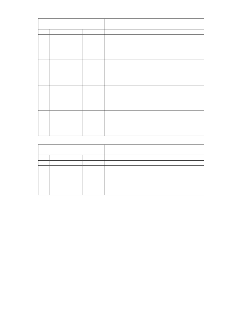
Table 60 –ATA Slew Rate Control A Register
ATA_SRCA
(0xE5 - RESET=0x00)
NAME
SLEW3
ATA SLEW RATE CONTROL A REGISTER
DESCRIPTION
These two bits are control inputs of the ATA pad for data
bits [15:12]. The bits can be used to vary the slew rate of
IDE_D[15:12] from minimum to maximum rate specified by
the ATA66 specification. The value 11b sets the slew rate
to be the maximum and the value of 00b sets the slew rate
to be the minimum.
These two bits are control inputs of the ATA pad for data
bits [11:8]. The bits can be used to vary the slew rate of
IDE_D[11:8] from minimum to maximum rate specified by
the ATA66 specification. The value 11b sets the slew rate
to be the maximum and the value of 00b sets the slew rate
to be the minimum.
These two bits are control inputs of the ATA pad for data
bits [7:4]. The bits can be used to vary the slew rate of
IDE_D[7:4] from minimum to maximum rate specified by the
ATA66 specification. The value 11b sets the slew rate to be
the maximum and the value of 00b sets the slew rate to be
the minimum.
These two bits are control inputs of the ATA pad for data
bits [3:0]. The bits can be used to vary the slew rate of
IDE_D[3:0] from minimum to maximum rate specified by the
ATA66 specification. The value 11b sets the slew rate to be
the maximum and the value of 00b sets the slew rate to be
the minimum.
BIT
[7:6]
R/W
R/W
[5:4]
SLEW2
R/W
[3:2]
SLEW1
R/W
[1:0]
SLEW0
R/W
Table 61 –ATA Slew Rate Control B Register
ATA_SRCB
(0xE6 - RESET=0x00)
NAME
Reserved
SLEW4
ATA SLEW RATE CONTROL B REGISTER
DESCRIPTION
Always returns “0” on reads
These two bits are control inputs of the ATA pad for
STROBE signaling during Ultra ATA writes to disk. The bits
can be used to vary the slew rate of STROBE from
minimum to maximum rate specified by the ATA66
specification. The value 11b sets the slew rate to be the
maximum and the value of 00b sets the slew rate to be the
minimum.
BIT
[7:2]
[1:0]
R/W
R
R/W
6.2 SIE Block
The SIE is a USB low-level protocol interpreter. The SIE controls the USB bus protocol, packet generation /
extraction, PID / Device ID parsing, and CRC coding / decodingwith autonomous error handling.
Parallel-to-serial / serial-to-parallel conversion, bit stuffing, and NRZI coding / decoding are handled in the PHY
block.
It is capable of operating either in USB 1.1 or 2.0 compliant modes. Unlike the normal 97Cxxx series SIEs, it has
more autonomous protocol handling functions like stall condition clearing on setup packets, suspend / resume / reset
conditions, and remote wakeup. It also autonomously handles the error conditions such as retry for CRC errors, Data
toggle errors, and generation of NYET, STALL, ACK and NACK depending on the endpoint buffer status.
During the power down state, the SIE clock is stopped. The SIE can asynchronously detect a USB Reset and/or
USB Resume condition and wakeup the 8051.
6.2.1
AUTONOMOUS USB PROTOCOL
相關(guān)PDF資料 |
PDF描述 |
|---|---|
| USH-1000-KS | Lamps for Photolithography |
| USH1000FAL2 | Lamps for Photolithography |
| USH1002FGL | Lamps for Photolithography |
| USH1002FNIL2 | Lamps for Photolithography |
| USH1002FNL | Lamps for Photolithography |
相關(guān)代理商/技術(shù)參數(shù) |
參數(shù)描述 |
|---|---|
| USB97CFDC2-01 | 制造商:SMSC 制造商全稱:SMSC 功能描述:USB Floppy Disk Controller |
| USB97CFDC2-MN-01 | 功能描述:USB 接口集成電路 USB Floppy Disk CNTRL RoHS:否 制造商:Cypress Semiconductor 產(chǎn)品:USB 2.0 數(shù)據(jù)速率: 接口類型:SPI 工作電源電壓:3.15 V to 3.45 V 工作電源電流: 最大工作溫度:+ 85 C 安裝風(fēng)格:SMD/SMT 封裝 / 箱體:WLCSP-20 |
| USB97CFDC2-MV-01 | 功能描述:USB 接口集成電路 USB Floppy Disk CNTRL RoHS:否 制造商:Cypress Semiconductor 產(chǎn)品:USB 2.0 數(shù)據(jù)速率: 接口類型:SPI 工作電源電壓:3.15 V to 3.45 V 工作電源電流: 最大工作溫度:+ 85 C 安裝風(fēng)格:SMD/SMT 封裝 / 箱體:WLCSP-20 |
| USB97CFDC2-MV-01X | 制造商:SMSC 制造商全稱:SMSC 功能描述:USB Floppy Disk Controller |
| USB97CFDC-MN | 制造商:Rochester Electronics LLC 功能描述:- Bulk 制造商:SMSC 功能描述: |
發(fā)布緊急采購,3分鐘左右您將得到回復(fù)。