- 您現(xiàn)在的位置:買賣IC網(wǎng) > PDF目錄384047 > USB2224 (SMSC Corporation) BUS POWERED USB2.0 FLASH MEDIA CONTROLLER PDF資料下載
參數(shù)資料
| 型號(hào): | USB2224 |
| 廠商: | SMSC Corporation |
| 英文描述: | BUS POWERED USB2.0 FLASH MEDIA CONTROLLER |
| 中文描述: | 總線供電個(gè)USB2.0閃存介質(zhì)控制器 |
| 文件頁數(shù): | 14/20頁 |
| 文件大?。?/td> | 286K |
| 代理商: | USB2224 |
Bus Powered USB2.0 Flash Media Controller
Datasheet
Revision 1.3 (09-21-04)
Page 14
SMSC USB2224
DATASHEET
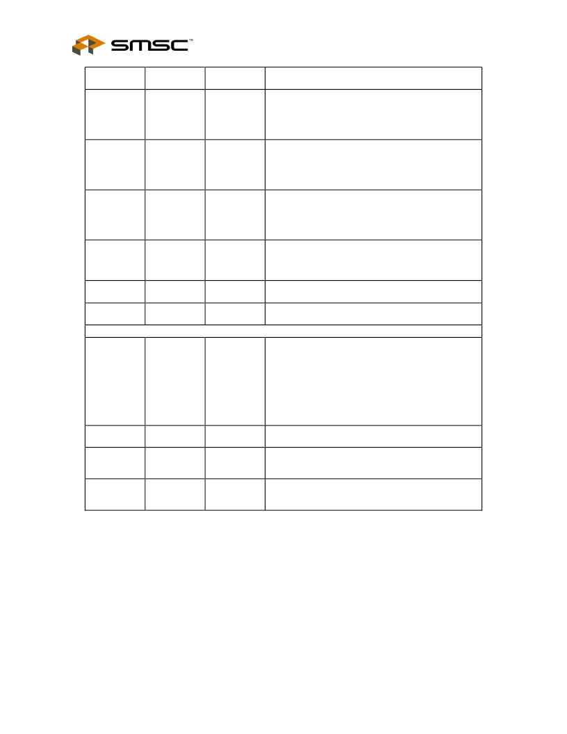
NAME
SYMBOL
BUFFER
TYPE
I/O8
DESCRIPTION
General
Purpose I/O
GPIO4
This pin may be used either as input, edge sensitive
interrupt input, or output.
This pin’s function while operating from internal ROM is
shown in Table 6.3 - GPIO Usage.
This pin may be used either as input, edge sensitive
interrupt input, or output.
This pin’s function while operating from internal ROM is
shown in Table 6.3 - GPIO Usage.
This pin may be used either as input, edge sensitive
interrupt input, or output.
This pin’s function while operating from internal ROM is
shown in Table 6.3 - GPIO Usage.
These pins may be used either as input, or output.
These pins’ functions while operating from internal ROM
are shown in Table 6.3 - GPIO Usage.
This active low signal is used by the system to reset the
chip. The active low pulse should be at least 1
μ
s wide.
These signals are used for testing the chip. User should
normally tie them high externally.
DIGITAL POWER, GROUNDS, and NO CONNECTS
VDDCORE
+1.8V Core power
All VDDCORE pins must be connected together on the
circuit board.
Pin 91 MUST have a 10uf +/- 20%, (equivalent series
resistance (ESR) <0.1ohm) bypass capacitor to VSSA,
and this capacitor should be placed as close to the pin as
possible.
VDDIO
+3.3V I/O power
General
Purpose I/O
GPIO5
I/O8
General
Purpose I/O
GPIO7
I/O8
General
Purpose I/O
GPIO[15:8]
I/O8
RESET input
nRESET
IS
TEST Input
nTEST[0:1]
I
1.8v Digital
Core Power
3.3v Digital I/O
power
VDDCORE
reference
ground
VDDIO
reference
ground
VSSCORE
VDDCORE ground Reference
VSSIO
VDDIO ground reference
Note 1:
Hot-insertion capable card connectors are required for all of flash medias. It is required for SD connector to
have Write Protect switch. This allows the chip to detect MMC card.
Note 2:
nMCE is normally asserted except when the system is in standby mode.
相關(guān)PDF資料 |
PDF描述 |
|---|---|
| USB2224-NE-02 | BUS POWERED USB2.0 FLASH MEDIA CONTROLLER |
| USB2224-NU-02 | BUS POWERED USB2.0 FLASH MEDIA CONTROLLER |
| USB2227 | 4TH GENERATION USB2.0 FLASH MEDIA CONTROLLER WITH INTEGRATED CARD POWER FETS |
| USB2227-NE-XX | 4TH GENERATION USB2.0 FLASH MEDIA CONTROLLER WITH INTEGRATED CARD POWER FETS |
| USB2227-NU-XX | 4TH GENERATION USB2.0 FLASH MEDIA CONTROLLER WITH INTEGRATED CARD POWER FETS |
相關(guān)代理商/技術(shù)參數(shù) |
參數(shù)描述 |
|---|---|
| USB2224_06 | 制造商:SMSC 制造商全稱:SMSC 功能描述:Bus Powered USB2.0 Flash Media Controller |
| USB2224-NE-02 | 制造商:Rochester Electronics LLC 功能描述:- Bulk |
| USB2224-NE-04 | 制造商:Rochester Electronics LLC 功能描述:- Bulk |
| USB2224-NE-05 | 制造商:Rochester Electronics LLC 功能描述:- Bulk |
| USB2224-NU-02 | 制造商:SMSC 制造商全稱:SMSC 功能描述:BUS POWERED USB2.0 FLASH MEDIA CONTROLLER |
發(fā)布緊急采購,3分鐘左右您將得到回復(fù)。