- 您現(xiàn)在的位置:買賣IC網(wǎng) > PDF目錄383984 > UPD8884ACY-A (NEC Corp.) (10680 PIXELS x 4 LINES) x 3 COLOR CCD LINEAR IMAGE SENSOR PDF資料下載
參數(shù)資料
| 型號: | UPD8884ACY-A |
| 廠商: | NEC Corp. |
| 英文描述: | (10680 PIXELS x 4 LINES) x 3 COLOR CCD LINEAR IMAGE SENSOR |
| 中文描述: | (1.068萬像素× 4行)× 3彩色CCD線性圖像傳感器 |
| 文件頁數(shù): | 6/28頁 |
| 文件大小: | 285K |
| 代理商: | UPD8884ACY-A |
第1頁第2頁第3頁第4頁第5頁當前第6頁第7頁第8頁第9頁第10頁第11頁第12頁第13頁第14頁第15頁第16頁第17頁第18頁第19頁第20頁第21頁第22頁第23頁第24頁第25頁第26頁第27頁第28頁
Data Sheet S17546EJ1V0DS
6
μ
PD8884A
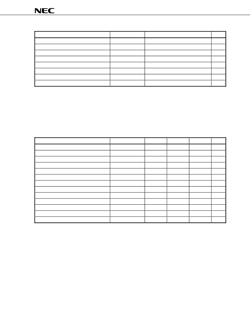
ABSOLUTE MAXIMUM RATINGS (T
A
=
+
25
°
C)
Parameter
Symbol
Ratings
Unit
Output drain voltage
V
OD
0.3 to
+
15
V
Shift register clock voltage
V
φ
1
, V
φ
2
0.3 to
+
8
V
Reset gate clock voltage
V
φ
RB
0.3 to
+
8
V
Reset feed-through level clamp clock voltage
V
φ
CLB
0.3 to
+
8
V
Dpi select signal voltage
V
φ
SEL1
to V
φ
SEL3
0.3 to
+
8
V
Transfer gate clock voltage
V
φ
TG1
to V
φ
TG3
0.3 to
+
8
V
Operating ambient temperature
Note
T
A
0 to
+
60
°
C
Storage temperature
T
stg
40 to
+
70
°
C
Note
Use at the condition without dew condensation.
Caution Product quality may suffer if the absolute maximum rating is exceeded even momentarily for any
parameter. That is, the absolute maximum ratings are rated values at which the product is on the
verge of suffering physical damage, and therefore the product must be used under conditions that
ensure that the absolute maximum ratings are not exceeded.
RECOMMENDED OPERATING CONDITIONS (T
A
=
+
25
°
C)
Parameter
Symbol
Min.
Typ.
Max.
Unit
Output drain voltage
V
OD
11.5
12.0
12.5
V
Shift register clock high level
V
φ
1H
, V
φ
2H
4.75
5.0
5.5
V
Shift register clock low level
V
φ
1L
, V
φ
2L
0.3
0
+
0.3
V
Reset gate clock high level
V
φ
RBH
4.5
5.0
5.5
V
Reset gate clock low level
V
φ
RBL
0.3
0
+
0.3
V
Reset feed-through level clamp clock high level
V
φ
CLBH
4.5
5.0
5.5
V
Reset feed-through level clamp clock low level
V
φ
CLBL
0.3
0
+
0.3
V
Dpi select signal high level
V
φ
SEL1H
to V
φ
SEL3H
4.5
5.0
5.5
V
Dpi select signal low level
V
φ
SEL1L
to V
φ
SEL3L
0.3
0
+
0.3
V
Transfer gate clock high level
V
φ
TG1H
to V
φ
TG3H
4.5
5.0
5.5
V
Transfer gate clock low level
V
φ
TG1L
to V
φ
TG3L
0.3
0
+
0.3
V
Data rate
f
φ
RB
2.0
5.0
MHz
Clock pulse frequency
f
φ
1
, f
φ
2
1.0
10.0
MHz
相關PDF資料 |
PDF描述 |
|---|---|
| UPD8884A | (10680 PIXELS x 4 LINES) x 3 COLOR CCD LINEAR IMAGE SENSOR |
| UPD8891 | (5340 x 5340) PIXELS x 3 + 2670 PIXELS x 3 COLOR CCD LINEAR IMAGE SENSOR |
| UPD8891CY | (5340 x 5340) PIXELS x 3 + 2670 PIXELS x 3 COLOR CCD LINEAR IMAGE SENSOR |
| UPD9611 | FOUR-CHANNEL PCM CODEC |
| UPD9611GT | FOUR-CHANNEL PCM CODEC |
相關代理商/技術參數(shù) |
參數(shù)描述 |
|---|---|
| UPD8891 | 制造商:NEC 制造商全稱:NEC 功能描述:(5340 x 5340) PIXELS x 3 + 2670 PIXELS x 3 COLOR CCD LINEAR IMAGE SENSOR |
| UPD8891CY | 制造商:Renesas Electronics Corporation 功能描述: |
| UPD89480GD-001-LML | 制造商:Renesas Electronics Corporation 功能描述: |
| UPD91000 | 制造商:未知廠家 制造商全稱:未知廠家 功能描述:Microcontroller |
| UPD92000 | 制造商:未知廠家 制造商全稱:未知廠家 功能描述:Microcontroller |
發(fā)布緊急采購,3分鐘左右您將得到回復。