- 您現(xiàn)在的位置:買賣IC網(wǎng) > PDF目錄384046 > UPD784916A (NEC Corp.) 16-BIT SINGLE-CHIP MICROCONTROLLERS PDF資料下載
參數(shù)資料
| 型號: | UPD784916A |
| 廠商: | NEC Corp. |
| 英文描述: | 16-BIT SINGLE-CHIP MICROCONTROLLERS |
| 中文描述: | 16位單晶片微控制器 |
| 文件頁數(shù): | 3/86頁 |
| 文件大小: | 446K |
| 代理商: | UPD784916A |
第1頁第2頁當(dāng)前第3頁第4頁第5頁第6頁第7頁第8頁第9頁第10頁第11頁第12頁第13頁第14頁第15頁第16頁第17頁第18頁第19頁第20頁第21頁第22頁第23頁第24頁第25頁第26頁第27頁第28頁第29頁第30頁第31頁第32頁第33頁第34頁第35頁第36頁第37頁第38頁第39頁第40頁第41頁第42頁第43頁第44頁第45頁第46頁第47頁第48頁第49頁第50頁第51頁第52頁第53頁第54頁第55頁第56頁第57頁第58頁第59頁第60頁第61頁第62頁第63頁第64頁第65頁第66頁第67頁第68頁第69頁第70頁第71頁第72頁第73頁第74頁第75頁第76頁第77頁第78頁第79頁第80頁第81頁第82頁第83頁第84頁第85頁第86頁
μ
PD784915A, 784916A
3
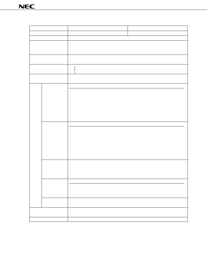
Function List (1/2)
Item
Internal ROM capacity
Internal RAM capacity
Operating clock
Minimum instruction ex-
ecution time
I/O ports
Real-time output port
Timer/counter
Capture register
VCR special circuit
General-purpose
timer
PWM output
Serial interface
A/D converter
μ
PD784915A
μ
PD784916A
48 Kbytes
1280 bytes
16 MHz (internal clock: 8 MHz)
Low frequency oscillation mode: 8 MHz (internal clock: 8 MHz)
Low power dissipation mode: 32.768 kHz (subsystem clock)
250 ns (with 8-MHz internal system clock)
64 Kbytes
input : 8
54
I/O
: 46
11 (including one each for pseudo V
SYNC
, head amplifier switch, and chrominance
rotation)
Timer/counter
Compare register
Capture register
TM0 (16 bits)
3
TM1 (16 bits)
3
FRC (22 bits)
-
TM3 (16 bits)
2
UDC (5 bits)
1
EC (8 bits)
4
EDV (8 bits)
1
Input signal
Number of bits
Measurable cycle
CFG
22
125 ns to 524 ms
DFG
22
125 ns to 524 ms
HSW
16
1
μ
s to 65.5 ms
V
SYNC
22
125 ns to 524 ms
CTL
16
1
μ
s to 65.5 ms
T
REEL
22
125 ns to 524 ms
S
REEL
22
125 ns to 524 ms
V
SYNC
separation circuit, H
SYNC
separation circuit
VISS detection, wide aspect detection circuits
Field identification circuit
Head amplifier switch/chroma rotation output circuit
Timer
Compare register
TM2 (16 bits)
1
TM4 (16 bits)
1 (capture/compare)
TM5 (16 bits)
1
16-bit accuracy : 3 channels (carrier frequency: 62.5 kHz)
8-bit accuracy
: 3 channels (carrier frequency: 62.5 kHz)
3-wire serial I/O: 2 channels
BUSY/STRB control (1 channel only)
8-bit resolution x 12 channels, conversion time: 10
μ
s
Remark
-
1
6
1
-
-
-
For HSW signal generation
For CFG signal division
Operating edge
↑
↑
↑
↑
↑
↑
↑
↓
↓
↓
↓
↓
Capture register
-
1
-
Super
timer
unit
相關(guān)PDF資料 |
PDF描述 |
|---|---|
| UPD784916AGF | 16-BIT SINGLE-CHIP MICROCONTROLLERS |
| UPD784915B | 16-BIT SINGLE-CHIP MICROCONTROLLERS |
| UPD784915BGF | 16-BIT SINGLE-CHIP MICROCONTROLLERS |
| UPD784916B | 16-BIT SINGLE-CHIP MICROCONTROLLERS |
| UPD784916BGF | 16-BIT SINGLE-CHIP MICROCONTROLLERS |
相關(guān)代理商/技術(shù)參數(shù) |
參數(shù)描述 |
|---|---|
| UPD784935AGF-113-3BA | 制造商:NEC Electronics Corporation 功能描述: |
| UPD784938AGF-188-3BA | 制造商:NEC Electronics Corporation 功能描述: |
| UPD789104AMC(A)-968-5A4-E2 | 制造商:Renesas Electronics Corporation 功能描述: |
| UPD789104AMC-671-5A4-E1 | 制造商:Renesas Electronics Corporation 功能描述: |
| UPD789104AMC-672-5A4-E1 | 制造商:Renesas Electronics Corporation 功能描述: |
發(fā)布緊急采購,3分鐘左右您將得到回復(fù)。