- 您現(xiàn)在的位置:買(mǎi)賣(mài)IC網(wǎng) > PDF目錄384046 > UPD784915A (NEC Corp.) 16-BIT SINGLE-CHIP MICROCONTROLLERS PDF資料下載
參數(shù)資料
| 型號(hào): | UPD784915A |
| 廠商: | NEC Corp. |
| 英文描述: | 16-BIT SINGLE-CHIP MICROCONTROLLERS |
| 中文描述: | 16位單晶片微控制器 |
| 文件頁(yè)數(shù): | 69/86頁(yè) |
| 文件大?。?/td> | 446K |
| 代理商: | UPD784915A |
第1頁(yè)第2頁(yè)第3頁(yè)第4頁(yè)第5頁(yè)第6頁(yè)第7頁(yè)第8頁(yè)第9頁(yè)第10頁(yè)第11頁(yè)第12頁(yè)第13頁(yè)第14頁(yè)第15頁(yè)第16頁(yè)第17頁(yè)第18頁(yè)第19頁(yè)第20頁(yè)第21頁(yè)第22頁(yè)第23頁(yè)第24頁(yè)第25頁(yè)第26頁(yè)第27頁(yè)第28頁(yè)第29頁(yè)第30頁(yè)第31頁(yè)第32頁(yè)第33頁(yè)第34頁(yè)第35頁(yè)第36頁(yè)第37頁(yè)第38頁(yè)第39頁(yè)第40頁(yè)第41頁(yè)第42頁(yè)第43頁(yè)第44頁(yè)第45頁(yè)第46頁(yè)第47頁(yè)第48頁(yè)第49頁(yè)第50頁(yè)第51頁(yè)第52頁(yè)第53頁(yè)第54頁(yè)第55頁(yè)第56頁(yè)第57頁(yè)第58頁(yè)第59頁(yè)第60頁(yè)第61頁(yè)第62頁(yè)第63頁(yè)第64頁(yè)第65頁(yè)第66頁(yè)第67頁(yè)第68頁(yè)當(dāng)前第69頁(yè)第70頁(yè)第71頁(yè)第72頁(yè)第73頁(yè)第74頁(yè)第75頁(yè)第76頁(yè)第77頁(yè)第78頁(yè)第79頁(yè)第80頁(yè)第81頁(yè)第82頁(yè)第83頁(yè)第84頁(yè)第85頁(yè)第86頁(yè)
μ
PD784915A, 784916A
69
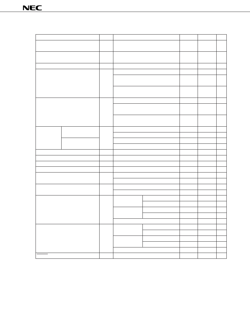
Other operations (T
A
= –10 to +70
°
C, V
DD
= AV
DD
= 4.5 to 5.5 V, V
SS
= AV
SS
= 0 V)
Parameter
Symbol
Condition
MIN.
MAX.
Unit
Timer input signal low-level width
t
WCTL
When DFGIN, CFGIN, DPGIN, REEL0IN,
t
CLK1
ns
or REEL1IN logic level is input
Timer input signal high-level width
t
WCTH
When DFGIN, CFGIN, DPGIN, REEL0IN,
t
CLK1
ns
or REEL1IN logic level is input
Timer input signal valid edge input cycle
t
PERIN
When DFGIN, CFGIN, or DPGIN is input
2
μ
s
CSYNCIN low-level width
t
WCR1L
When digital noise elimination circuit is not used
8t
CLK1
ns
When digital noise elimination circuit is used
108t
CLK1
ns
(Bit 4 of INTM2 = 0)
When digital noise elimination circuit is used
180t
CLK1
ns
(Bit 4 of INTM2 = 1)
CSYNCIN high-level width
t
WCR1H
When digital noise elimination circuit is not used
8t
CLK1
ns
When digital noise elimination circuit is used
108t
CLK1
ns
(Bit 4 of INTM2 = 0)
When digital noise elimination circuit is used
180t
CLK1
ns
(Bit 4 of INTM2 = 1)
Digital noise
Eliminated pulse width
t
WSEP
Bit 4 of INTM2 = 0
104t
CLK1
ns
elimination
Bit 4 of INTM2 = 1
176t
CLK1
ns
circuit
Passed pulse width
Bit 4 of INTM2 = 0
108t
CLK1
ns
Bit 4 of INTM2 = 1
180t
CLK1
ns
NMI low-level width
t
WNIL
V
DD
= AV
DD
= 2.7 to 5.5 V
10
μ
s
μ
s
NMI high-level width
t
WNIH
V
DD
= AV
DD
= 2.7 to 5.5 V
10
INTP0, INTP3 low-level widths
t
WIPL0
2t
CLK1
ns
INTP0, INTP3 high-level widths
t
WIPH0
2t
CLK1
ns
INTP1, KEY0-KEY4 low-level widths
t
WIPL1
Mode other than STOP mode
2t
CLK1
ns
In STOP mode, for releasing STOP mode
10
μ
s
INTP1, KEY0-KEY4 high-level widths
t
WIPH1
Mode other than STOP mode
2t
CLK1
ns
In STOP mode, for releasing STOP mode
10
μ
s
INTP2 low-level width
t
WIPL2
In normal mode,
Sampling = f
CLK
2t
CLK1
32
Note
ns
with main clock
Sampling = f
CLK
/128
μ
s
μ
s
Normal mode,
Sampling = f
CLK
61
with subclock
Sampling = f
CLK
/128
7.9
Note
ms
In STOP mode, for releasing STOP mode
10
μ
s
INTP2 high-level width
t
WIPH2
In normal mode,
Sampling = f
CLK
2t
CLK1
32
Note
ns
with main clock
Sampling = f
CLK
/128
μ
s
μ
s
Normal mode,
Sampling = f
CLK
61
with subclock
Sampling = f
CLK
/128
7.9
Note
ms
In STOP mode, for releasing STOP mode
10
μ
s
μ
s
RESET low-level width
t
WRSL
10
Note
If a high or low level is successively input two times during the sampling period, a high or low level is
detected.
Remark
t
CKL1
: operating clock cycle time of peripheral circuit (125 ns)
相關(guān)PDF資料 |
PDF描述 |
|---|---|
| UPD784915AGF | 16-BIT SINGLE-CHIP MICROCONTROLLERS |
| UPD784916A | 16-BIT SINGLE-CHIP MICROCONTROLLERS |
| UPD784916AGF | 16-BIT SINGLE-CHIP MICROCONTROLLERS |
| UPD784915B | 16-BIT SINGLE-CHIP MICROCONTROLLERS |
| UPD784915BGF | 16-BIT SINGLE-CHIP MICROCONTROLLERS |
相關(guān)代理商/技術(shù)參數(shù) |
參數(shù)描述 |
|---|---|
| UPD784935AGF-113-3BA | 制造商:NEC Electronics Corporation 功能描述: |
| UPD784938AGF-188-3BA | 制造商:NEC Electronics Corporation 功能描述: |
| UPD789104AMC(A)-968-5A4-E2 | 制造商:Renesas Electronics Corporation 功能描述: |
| UPD789104AMC-671-5A4-E1 | 制造商:Renesas Electronics Corporation 功能描述: |
| UPD789104AMC-672-5A4-E1 | 制造商:Renesas Electronics Corporation 功能描述: |
發(fā)布緊急采購(gòu),3分鐘左右您將得到回復(fù)。