- 您現(xiàn)在的位置:買賣IC網(wǎng) > PDF目錄384046 > UPD780033AYCW (NEC Corp.) 8-BIT SINGLE-CHIP MICROCONTROLLERS PDF資料下載
參數(shù)資料
| 型號(hào): | UPD780033AYCW |
| 廠商: | NEC Corp. |
| 元件分類: | 8位微控制器 |
| 英文描述: | 8-BIT SINGLE-CHIP MICROCONTROLLERS |
| 中文描述: | 8位單晶片微控制器 |
| 文件頁(yè)數(shù): | 40/70頁(yè) |
| 文件大小: | 527K |
| 代理商: | UPD780033AYCW |
第1頁(yè)第2頁(yè)第3頁(yè)第4頁(yè)第5頁(yè)第6頁(yè)第7頁(yè)第8頁(yè)第9頁(yè)第10頁(yè)第11頁(yè)第12頁(yè)第13頁(yè)第14頁(yè)第15頁(yè)第16頁(yè)第17頁(yè)第18頁(yè)第19頁(yè)第20頁(yè)第21頁(yè)第22頁(yè)第23頁(yè)第24頁(yè)第25頁(yè)第26頁(yè)第27頁(yè)第28頁(yè)第29頁(yè)第30頁(yè)第31頁(yè)第32頁(yè)第33頁(yè)第34頁(yè)第35頁(yè)第36頁(yè)第37頁(yè)第38頁(yè)第39頁(yè)當(dāng)前第40頁(yè)第41頁(yè)第42頁(yè)第43頁(yè)第44頁(yè)第45頁(yè)第46頁(yè)第47頁(yè)第48頁(yè)第49頁(yè)第50頁(yè)第51頁(yè)第52頁(yè)第53頁(yè)第54頁(yè)第55頁(yè)第56頁(yè)第57頁(yè)第58頁(yè)第59頁(yè)第60頁(yè)第61頁(yè)第62頁(yè)第63頁(yè)第64頁(yè)第65頁(yè)第66頁(yè)第67頁(yè)第68頁(yè)第69頁(yè)第70頁(yè)
40
μ
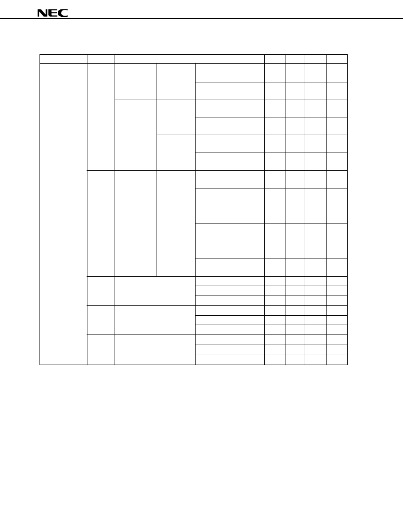
PD780031AY, 780032AY, 780033AY, 780034AY
Data Sheet U14045EJ1V0DS00
DC Characteristics (T
A
= –40 to +85
°
C, V
DD
= 1.8 to 5.5 V)
Parameter
Symbol
Test Conditions
MIN.
TYP.
MAX.
Unit
Power supply
current
Note 1
I
DD1
8.38-MHz
crystal oscillation
operating mode
V
DD
= 5.0V
±
10%
Note 2
When A/D converter is
stopped
5.5
11
mA
When A/D converter is
operating
6.5
13
mA
5.00-MHz
crystal oscillation
operating mode
V
DD
= 3.0V
±
10%
Note 2
When A/D converter is
stopped
2
4
mA
When A/D converter is
operating
3
6
mA
V
DD
= 2.0V
±
10%
Note 3
When A/D converter is
stopped
0.4
1.5
mA
When A/D converter is
operating
1.4
4.2
mA
I
DD2
8.38-MHz
crystal oscillation
HALT mode
V
DD
= 5.0V
±
10%
Note 2
When peripheral functions
are stopped
1.1
2.2
mA
When peripheral functions
are operating
4.7
mA
5.00-MHz
crystal oscillation
HALT mode
V
DD
= 3.0V
±
10%
Note 2
When peripheral functions
are stopped
0.35
0.7
mA
When peripheral functions
are operating
1.7
mA
V
DD
= 2.0V
±
10%
Note 3
When peripheral functions
are stopped
0.15
0.4
mA
When peripheral functions
are operating
1.1
mA
I
DD3
32.768-kHz crystal oscillation
operating mode
Note 4
V
DD
= 5.0 V
±
10%
40
80
μ
A
V
DD
= 3.0 V
±
10%
20
40
μ
A
V
DD
= 2.0 V
±
10%
10
20
μ
A
I
DD4
32.768-kHz crystal oscillation
HALT mode
Note 4
V
DD
= 5.0 V
±
10%
30
60
μ
A
V
DD
= 3.0 V
±
10%
6
18
μ
A
V
DD
= 2.0 V
±
10%
2
10
μ
A
I
DD5
XT1 = 0V STOP mode
When feedback resistor is not used
V
DD
= 5.0 V
±
10%
0.1
30
μ
A
V
DD
= 3.0 V
±
10%
0.05
10
μ
A
V
DD
= 2.0 V
±
10%
0.05
10
μ
A
Notes 1.
Total current through the internal power supply (V
DD0
, V
DD1
), including the peripheral operation current
(except the current through pull-up resistors of ports and the AV
REF
pin).
2.
When the processor clock control register (PCC) is set to 00H.
3.
When PCC is set to 02H.
4.
When main system clock operation is stopped.
相關(guān)PDF資料 |
PDF描述 |
|---|---|
| UPD780033AYGC | 8-BIT SINGLE-CHIP MICROCONTROLLERS |
| UPD780033AYGK | 8-BIT SINGLE-CHIP MICROCONTROLLERS |
| UPD780226 | MOS INTERGRATED CIRCUIT |
| UPD780226GF | MOS INTERGRATED CIRCUIT |
| UPD780226GF-xxx-3BA | MOS INTERGRATED CIRCUIT |
相關(guān)代理商/技術(shù)參數(shù) |
參數(shù)描述 |
|---|---|
| UPD780034AGC-119-8BS-A | 制造商:Renesas Electronics Corporation 功能描述:NECUPD780034AGC-119-8BS-A MCU |
| UPD780053GC-055-8BT-A | 制造商:Renesas Electronics Corporation 功能描述: |
| UPD780101MC-047-5A4-E1-A | 制造商:Renesas Electronics Corporation 功能描述: |
| UPD780102MC-082-5A4-A | 制造商:Renesas Electronics Corporation 功能描述: |
| UPD780102MC-083-5A4-A | 制造商:Renesas Electronics Corporation 功能描述: |
發(fā)布緊急采購(gòu),3分鐘左右您將得到回復(fù)。