- 您現(xiàn)在的位置:買賣IC網(wǎng) > PDF目錄384045 > UPD72873 (NEC Corp.) MOS INTEGRATED CIRCUIT PDF資料下載
參數(shù)資料
| 型號(hào): | UPD72873 |
| 廠商: | NEC Corp. |
| 英文描述: | MOS INTEGRATED CIRCUIT |
| 中文描述: | 馬鞍山集成電路 |
| 文件頁數(shù): | 24/40頁 |
| 文件大小: | 269K |
| 代理商: | UPD72873 |
第1頁第2頁第3頁第4頁第5頁第6頁第7頁第8頁第9頁第10頁第11頁第12頁第13頁第14頁第15頁第16頁第17頁第18頁第19頁第20頁第21頁第22頁第23頁當(dāng)前第24頁第25頁第26頁第27頁第28頁第29頁第30頁第31頁第32頁第33頁第34頁第35頁第36頁第37頁第38頁第39頁第40頁
Preliminary Data Sheet S15305EJ2V0DS
24
μ
PD72873
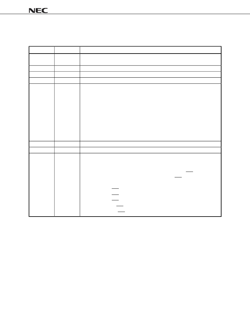
3.1.21 Offset_62 Power Management Capabilities Register
This is a 16-bit read-only register that provides information on the power management capabilities of the
μ
PD72873.
Bits
R/W
Description
2-0
R
Version
Constant value of 010. The power management registers are implemented as
defined in revision 1.1 of PCI Bus Power Management Interface Specification.
3
R
PME clock
Constant value of 0.
4
R
Reserved
Constant value of 0.
5
R
DSI
Constant value of 0.
8-6
R
Auxiliary Power
Default value of 000. This field reports the Vaux power requirements for the
μ
PD72873. This data is programable from EEPROM.
111 – 375 mA maximum current required for a 3.3 Vaux,
110 – 320 mA maximum current required for a 3.3 Vaux,
101 – 270 mA maximum current required for a 3.3 Vaux,
100 – 220 mA maximum current required for a 3.3 Vaux,
011 – 160 mA maximum current required for a 3.3 Vaux,
010 – 100 mA maximum current required for a 3.3 Vaux,
001 – 55 mA maximum current required for a 3.3 Vaux,
000 – 0 (self powered)
9
R
D1_support
Constant value of 1. The
μ
PD72873 supports the D1 Power Management state.
10
R
D2_support
Constant value of 1. The
μ
PD72873 supports the D2 Power Management state.
15-11
R
PME_support
D3SUP = ‘High’ : Constant value of 11111.
D3SUP = ‘Low’ : Constant value of 01111.
This field indicates the power states in which the
μ
PD72873 may assert PME. A value of “0” for
any bit indicates that the function is not capable of asserting the PME signal while in that power
state.
bit (11) – PME_D0. PME can be asserted from D0.
bit (12) – PME_D1. PME can be asserted from D1.
bit (13) – PME_D2. PME can be asserted from D2.
bit (14) – PME_D3hot. PME can be asserted from D3hot.
bit (15) – PME_D3cold. PME can be asserted from D3cold.
相關(guān)PDF資料 |
PDF描述 |
|---|---|
| UPD72873GC-YEB | MOS INTEGRATED CIRCUIT |
| UPD72874 | IEEE1394 OHCI 1.1 COMPLIANT 3PORT PHY-LINK 1-CHIP HOST CONTROLLER |
| UPD72874GC-YEB | IEEE1394 OHCI 1.1 COMPLIANT 3PORT PHY-LINK 1-CHIP HOST CONTROLLER |
| UPD7281 | IEEE1394 OHCI 1.1 COMPLIANT 3PORT PHY-LINK 1-CHIP HOST CONTROLLER |
| UPD753036 | 4-BIT SINGLE-CHIP MICROCONTROLLER FOR SMALL GENERAL-PURPOSE INFRARED REMOTE CONTROL TRANSMITTER |
相關(guān)代理商/技術(shù)參數(shù) |
參數(shù)描述 |
|---|---|
| UPD74HC04C | 制造商:Panasonic Industrial Company 功能描述:IC |
| UPD750068GT-396 | 制造商:Renesas Electronics Corporation 功能描述: |
| UPD7507C189 | 制造商:Panasonic Industrial Company 功能描述:IC |
| UPD7508CU265 | 制造商:Panasonic Industrial Company 功能描述:IC |
| UPD75208 | 制造商:Panasonic Industrial Company 功能描述:IC |
發(fā)布緊急采購,3分鐘左右您將得到回復(fù)。