- 您現(xiàn)在的位置:買賣IC網(wǎng) > PDF目錄383980 > UPD16837 (NEC Corp.) MONOLITHIC QUAD H BRIDGE DRIVER PDF資料下載
參數(shù)資料
| 型號: | UPD16837 |
| 廠商: | NEC Corp. |
| 英文描述: | MONOLITHIC QUAD H BRIDGE DRIVER |
| 中文描述: | 單片四H橋驅(qū)動 |
| 文件頁數(shù): | 2/16頁 |
| 文件大小: | 110K |
| 代理商: | UPD16837 |
μ
PD16837
2
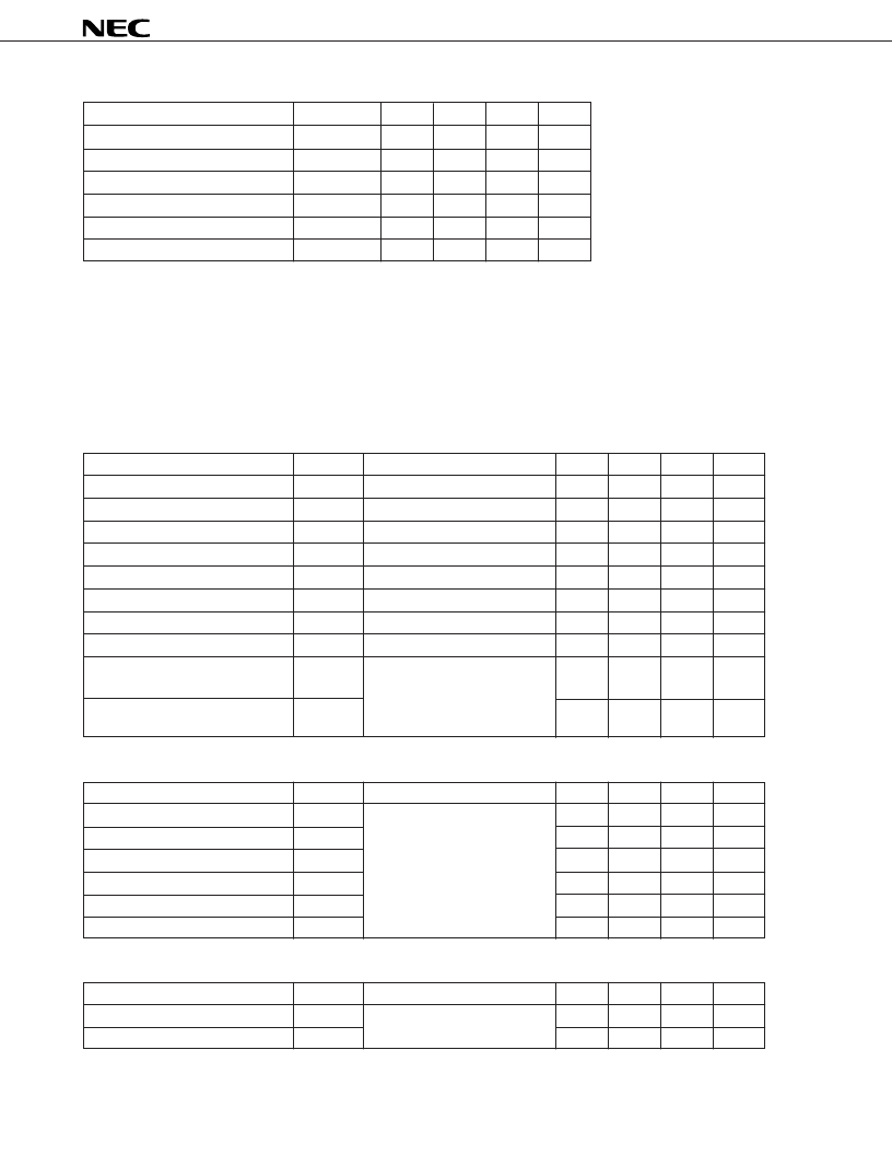
RECOMMENDED OPERATING RANGE
Parameter
Symbol
MIN.
TYP.
MAX.
Unit
Control block supply voltage
V
DD
Note 1
4.0
5.0
6.0
V
Output block supply voltage
V
M
10.8
12.0
13.2
V
H bridge drive current
I
DR (pulse)
Note 2
–600
600
mA
Operating frequency
f
O
120
kHz
Operating temperature range
T
A
0
75
°
C
Peak junction temperature
T
CH (MAX)
125
°
C
Notes 1.
The low-voltage malfunction prevention circuit operates when V
DD
is 1.5 V or higher but less than 4 V
(2.5 V TYP.).
2.
PW
≤
5 ms, Duty
≤
10%
ELECTRICAL CHARACTERISTICS (T
A
= 25
°
C)
T
A
= 25
°
C and the other parameters are within their recommended operating ranges as described above
unless otherwise specified.
The parameters other than changes in delay time are when the current is ON.
The low-voltage malfunction prevention circuit operates when V
DD
is 1.5 V to 4 V.
Parameter
Symbol
Conditions
MIN.
TYP.
MAX.
Unit
V
M
pin current (leakage current)
I
M
V
M
= 13.2 V
50
μ
A
V
DD
pin current
I
DD
V
DD
= 6 V
200
μ
A
High-level input current
I
IH
V
IN
= V
DD
0.25
mA
Low-level input current
I
IL
V
IN
= 0
–2.0
μ
A
High-level input voltage
Note 1
V
IH
V
DD
= 5 V, V
M
= 12 V
3.0
V
DD
+ 0.3
V
Low-level input voltage
Note 1
V
IL
V
DD
= 5 V, V
M
= 12 V
–0.3
0.8
V
H bridge ON resistance (chs 2 and 3)
R
ONa
V
DD
= 5 V, V
M
= 12 V
3.0
4.0
H bridge ON resistance (chs 1 and 4)
R
ONb
V
DD
= 5 V, V
M
= 12 V
1.5
2.0
H bridge switching current without
load (chs 2 and 3)
Note 2
I
sa (AVE)
V
DD
= 5 V
3.0
mA
V
M
= 12 V
H bridge switching current without
load (chs 1 and 4)
Note 2
I
sb (AVE)
at 100 kHz
4.5
mA
ch2, ch3 2A, 3A, 2B, 3B Output
Parameter
Symbol
Conditions
MIN.
TYP.
MAX.
Unit
Rise time
t
TLHa
V
DD
= 5 V
200
ns
Rising delay time
t
PLHa
V
M
= 12 V
350
ns
Change in rising delay time
t
PLHa
20
110
ns
Fall time
t
THLa
at 100 kHz
200
ns
Falling delay time
t
PHLa
350
ns
Change in falling delay time
t
PHLa
130
ns
ch2, ch3 2A-2B, 3A-3B
Parameter
Symbol
Conditions
MIN.
TYP.
MAX.
Unit
Rising delay time differential
t
PLHa (A-B)
V
DD
= 5 V, V
M
= 12 V
50
ns
Falling delay time differential
t
PHLa (A-B)
20
at 100kHz
50
ns
Notes 1.
The input pins are the IN and SEL pins.
2.
Average value of the current consumed internally by an H bridge circuit when the circuit is switched without
load.
相關(guān)PDF資料 |
PDF描述 |
|---|---|
| UPD16837GS | MONOLITHIC QUAD H BRIDGE DRIVER |
| UPD16855A | DUAL HIGH-SIDE SWITCH FOR USB APPLICATION |
| UPD16855AG | DUAL HIGH-SIDE SWITCH FOR USB APPLICATION |
| UPD16855BC | DUAL HIGH-SIDE SWITCH FOR USB APPLICATION |
| UPD16855BG | DUAL HIGH-SIDE SWITCH FOR USB APPLICATION |
相關(guān)代理商/技術(shù)參數(shù) |
參數(shù)描述 |
|---|---|
| UPD16837GS | 制造商:Renesas Electronics Corporation 功能描述: |
| UPD16855 | 制造商:未知廠家 制造商全稱:未知廠家 功能描述:Analog IC |
| UPD16855A | 制造商:NEC 制造商全稱:NEC 功能描述:DUAL HIGH-SIDE SWITCH FOR USB APPLICATION |
| UPD16855AG | 制造商:NEC 制造商全稱:NEC 功能描述:DUAL HIGH-SIDE SWITCH FOR USB APPLICATION |
| UPD16855B | 制造商:未知廠家 制造商全稱:未知廠家 功能描述:UPD16855A/B/C/D Data Sheet | Data Sheet[02/1999] |
發(fā)布緊急采購,3分鐘左右您將得到回復(fù)。