- 您現(xiàn)在的位置:買(mǎi)賣(mài)IC網(wǎng) > PDF目錄383979 > UPD16664 (NEC Corp.) 144/160/184/208-OUTPUT LCD COLUMN SEGMENT DRIVER WITH RAM PDF資料下載
參數(shù)資料
| 型號(hào): | UPD16664 |
| 廠商: | NEC Corp. |
| 英文描述: | 144/160/184/208-OUTPUT LCD COLUMN SEGMENT DRIVER WITH RAM |
| 中文描述: | 144/160/184/208-OUTPUT液晶柱段驅(qū)動(dòng)與RAM |
| 文件頁(yè)數(shù): | 2/52頁(yè) |
| 文件大小: | 347K |
| 代理商: | UPD16664 |
第1頁(yè)當(dāng)前第2頁(yè)第3頁(yè)第4頁(yè)第5頁(yè)第6頁(yè)第7頁(yè)第8頁(yè)第9頁(yè)第10頁(yè)第11頁(yè)第12頁(yè)第13頁(yè)第14頁(yè)第15頁(yè)第16頁(yè)第17頁(yè)第18頁(yè)第19頁(yè)第20頁(yè)第21頁(yè)第22頁(yè)第23頁(yè)第24頁(yè)第25頁(yè)第26頁(yè)第27頁(yè)第28頁(yè)第29頁(yè)第30頁(yè)第31頁(yè)第32頁(yè)第33頁(yè)第34頁(yè)第35頁(yè)第36頁(yè)第37頁(yè)第38頁(yè)第39頁(yè)第40頁(yè)第41頁(yè)第42頁(yè)第43頁(yè)第44頁(yè)第45頁(yè)第46頁(yè)第47頁(yè)第48頁(yè)第49頁(yè)第50頁(yè)第51頁(yè)第52頁(yè)
Data Sheet S13780EJ1V0DS00
2
μ
PD16664
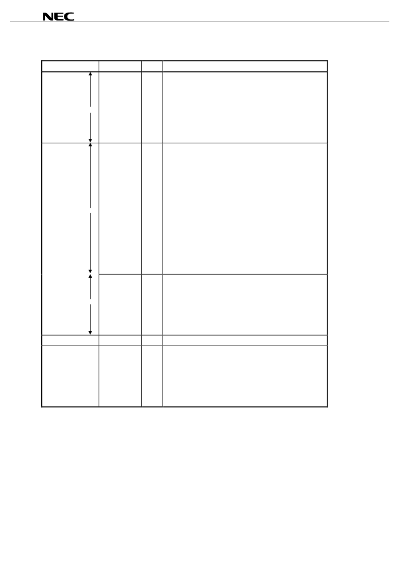
1. PIN NAME
Classification
Pin Name
Note
I/O
Function
CPU interface
V
CC2
D
0
-D
15
A
0
-A
16
/CS
/OE
/WE
/UBE
RDY
I/O
I
I
I
I
I
O
Data bus: 16 bits
Address bus: 17 bits
Chip select
Read signal
Write signal
Upper byte enable
Ready signal to CPU (“H”: ready)
Control signals
V
CC2
PL0
PL1
DIR
DMODE
CMODE0,1
MS
BMODE
/REFRH
TEST
/RESET
/DOFF
OSC1
OSC2
I
I
I
I
I
I
I
I/O
I
I
I
–
–
Specifies LSI layout position (No. 0 to 3)
Specifies LSI layout position (No. 0 to 3)
Specifies liquid crystal panel layout position
Duty selection (“H” = 1/128 duty, “L” =1/160 duty)
Number of column outputs selection
Master/slave selection (“H”: master mode)
Data bus bit selection (“H” = 8 bits, “L” = 16 bits)
Self-diagnosis reset pin (wired-OR connection)
Test pin (“H” = test mode, with pull-down resistor)
Reset signal
Display OFF input signal
External resistor pin for oscillator
External resistor pin for oscillator
V
CC1
STB
/FRM
PULSE
L1
L2
/DOUT
I/O
I/O
I/O
I/O
I/O
O
Column drive signal (MS pin “H” = output, MS pin “L” = input)
Frame signal (MS pin “H” = output, MS pin “L” = input)
25-level pulse modulation clock
Row driver drive level select signal (first line)
Row driver drive level select signal (second line)
Display OFF output signal
Liquid crystal drive
Y
1
-Y
208
O
Liquid crystal drive output
Power
GND
V
CC1
V
CC2
V
0
V
1
V
2
–
–
–
–
–
–
Ground (two pins for V
CC1
system, three pins for V
CC2
system)
Power supply for liquid crystal drive and row driver interface
Power supply for logic
Liquid crystal drive analog power
Liquid crystal drive analog power
Liquid crystal drive analog power
Note
V
CC2
system pins : D
0
to D
15
, A
0
to A
16
, /CS, /OE, /WE, /UBE, RDY, BMODE, PL0, PL1, DIR,
OSC1, OSC2, /RESET, /DOFF, TEST, MS, CMODE0, CMODE1, DMODE
V
CC1
system pins : STB, /FRM, L1, L2, /DOUT, PULSE
Remark
/xxx indicates active low signals.
相關(guān)PDF資料 |
PDF描述 |
|---|---|
| UPD16682 | CONN CABLE CLAMP METAL #18 IP68 |
| UPD16682N | 1/65 DUTY LCD CONTROLLER/DRIVER WITH ON-CHIP RAM |
| UPD16682P | 1/65 DUTY LCD CONTROLLER/DRIVER WITH ON-CHIP RAM |
| UPD16682W | 1/65 DUTY LCD CONTROLLER/DRIVER WITH ON-CHIP RAM |
| UPD16700 | 256-OUTPUT TFT-LCD GATE DRIVER |
相關(guān)代理商/技術(shù)參數(shù) |
參數(shù)描述 |
|---|---|
| UPD16664N | 制造商:NEC 制造商全稱(chēng):NEC 功能描述:144/160/184/208-OUTPUT LCD COLUMN SEGMENT DRIVER WITH RAM |
| UPD16664N-001 | 制造商:NEC 制造商全稱(chēng):NEC 功能描述:144/160/184/208-OUTPUT LCD COLUMN SEGMENT DRIVER WITH RAM |
| UPD16664N-XXX | 制造商:未知廠家 制造商全稱(chēng):未知廠家 功能描述:LCD Display Driver |
| UPD16666A | 制造商:NEC 制造商全稱(chēng):NEC 功能描述:240-OUTPUT LCD ROW DRIVER |
| UPD16666AN | 制造商:NEC 制造商全稱(chēng):NEC 功能描述:240-OUTPUT LCD ROW DRIVER |
發(fā)布緊急采購(gòu),3分鐘左右您將得到回復(fù)。