- 您現(xiàn)在的位置:買賣IC網(wǎng) > PDF目錄383979 > UPD16650 (NEC Corp.) 120-/128-OUTPUT TFT-LCD GATE DRIVER PDF資料下載
參數(shù)資料
| 型號: | UPD16650 |
| 廠商: | NEC Corp. |
| 英文描述: | 120-/128-OUTPUT TFT-LCD GATE DRIVER |
| 中文描述: | 120-/128-OUTPUT的TFT - LCD柵極驅(qū)動器 |
| 文件頁數(shù): | 5/12頁 |
| 文件大小: | 62K |
| 代理商: | UPD16650 |
μ
PD16650
5
CAUTIONS FOR USE
1)
Power-on sequence
To prevent latch-up disruption, the power must be switched on in the order:
V
CC
→
V
EE1
→
V
EE2
→
V
DD
→
Logic input
When witching off, reverse the order. This order must be observed also during transition.
2)
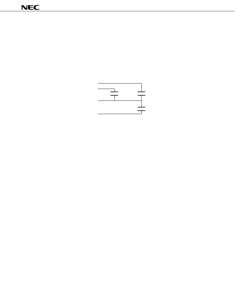
Insertion of bypass capacitors
The internal logic circuit operates at a high voltage. To make V
IH
and V
IL
immune to noise, use capacitors of
0.1
μ
F or so between supply voltages as shown below.
V
DD
V
CC
V
SS
V
EE2
0.1 F
0.1 F
0.1 F
3)
Negative voltage level shift
If it is necessary to shift the level of a negative supply voltage, shift the V
EE1
(driver supply voltage) level. The
shift should be limited to within: V
EE2
≤
V
EE1
≤
V
EE2
+ 10 V
Note that shifting the V
EE1
level results in the ON-state output resistance and output fall time ratings being
changed.
4)
Handling the V
EE1
and V
EE2
driver negative supply voltage pins
For applications in which a negative supply voltage level is not shifted, connect the V
EE1
pin (driver supply voltage)
to the V
EE2
pin (logic supply voltage) outside the TCP. Fix all unused input pins to the V
EE2
level.
相關PDF資料 |
PDF描述 |
|---|---|
| UPD16650N | 120-/128-OUTPUT TFT-LCD GATE DRIVER |
| UPD16655N-XXX | LCD Display Driver |
| UPD16655 | 240-OUTPUT TFT-LCD GATE DRIVER |
| UPD16655N | 240-OUTPUT TFT-LCD GATE DRIVER |
| UPD16664N-001 | 144/160/184/208-OUTPUT LCD COLUMN SEGMENT DRIVER WITH RAM |
相關代理商/技術參數(shù) |
參數(shù)描述 |
|---|---|
| UPD16650N | 制造商:NEC 制造商全稱:NEC 功能描述:120-/128-OUTPUT TFT-LCD GATE DRIVER |
| UPD16650N-XXX | 制造商:NEC 制造商全稱:NEC 功能描述:Interface IC |
| UPD16652N-XXX | 制造商:未知廠家 制造商全稱:未知廠家 功能描述:LCD Display Driver |
| UPD16654 | 制造商:NEC 制造商全稱:NEC 功能描述:150/154 OUTPUT TFT-LCD GATE DRIVE |
| UPD16654N | 制造商:NEC 制造商全稱:NEC 功能描述:150/154 OUTPUT TFT-LCD GATE DRIVE |
發(fā)布緊急采購,3分鐘左右您將得到回復。