- 您現(xiàn)在的位置:買賣IC網(wǎng) > PDF目錄384038 > UPA2706TP (NEC Corp.) SWITCHING N-CHANNEL POWER MOSFET PDF資料下載
參數(shù)資料
| 型號: | UPA2706TP |
| 廠商: | NEC Corp. |
| 英文描述: | SWITCHING N-CHANNEL POWER MOSFET |
| 中文描述: | 開關N溝道功率MOSFET |
| 文件頁數(shù): | 1/7頁 |
| 文件大?。?/td> | 78K |
| 代理商: | UPA2706TP |
The information in this document is subject to change without notice. Before using this document, please
confirm that this is the latest version.
Not all products and/or types are available in every country. Please check with an NEC Electronics
sales representative for availability and additional information.
MOS FIELD EFFECT TRANSISTOR
μ
PA2706GR
SWITCHING
N-CHANNEL POWER MOS FET
DATA SHEET
Document No. G16236EJ1V0DS00 (1st edition)
Date Published April 2003 NS CP(K)
Printed in Japan
2003
DESCRIPTION
The
μ
PA2706GR is N-Channel MOS Field Effect Transistor
designed for DC/DC converters and power management
applications of notebook computers.
FEATURES
Low on-state resistance
R
DS(on)1
= 15 m
MAX. (V
GS
= 10 V, I
D
= 5.5 A)
R
DS(on)2
= 22.5 m
MAX. (V
GS
= 4.5 V, I
D
= 5.5 A)
Low C
iss
: C
iss
= 660 pF TYP. (V
DS
= 10 V, V
GS
= 0 V)
Small and surface mount package (Power SOP8)
ORDERING INFORMATION
PART NUMBER
PACKAGE
μ
PA2706GR
Power SOP8
ABSOLUTE MAXIMUM RATINGS (T
A
= 25°C, All terminals are connected)
Drain to Source Voltage (V
GS
= 0 V)
Gate to Source Voltage (V
DS
= 0 V)
Drain Current (DC)
Drain Current (pulse)
Note1
Total Power Dissipation (T
A
= 25°C)
Note2
V
DSS
V
GSS
I
D(DC)
I
D(pulse)
P
T
T
ch
T
stg
I
AS
E
AS
30
±
20
±
11
±
44
2.0
150
V
V
A
A
W
°C
°C
A
mJ
Channel Temperature
Storage Temperature
Single Avalanche Current
Note3
Single Avalanche Energy
Note3
55 to + 150
11
12.1
Notes 1.
PW
≤
10
μ
s, Duty Cycle
≤
1%
2.
Mounted on ceramic substrate of 1200 mm
2
x 2.2 mm
3.
Starting T
ch
= 25°C, V
DD
= 15 V, R
G
= 25
, L = 100
μ
H, V
GS
= 20
→
0 V
Caution
Strong electric field, when exposed to this device, can cause destruction of the gate oxide and ultimately
degrade the device operation. Steps must be taken to stop generation of static electricity as much as
possible, and quickly dissipate it once, when it has occurred.
Remark
The diode connected between the gate and source of the transistor serves as a protector against ESD.
When this device actually used, an additional protection circuit is externally required if a voltage exceeding
the rated voltage may be applied to this device.
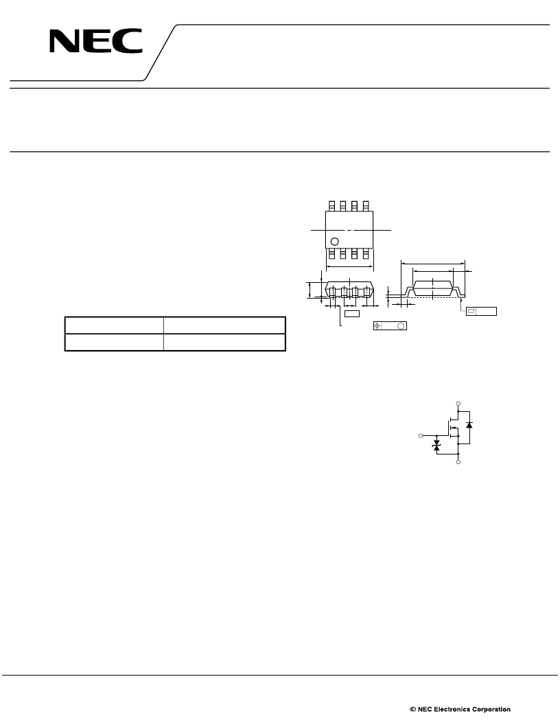
PACKAGE DRAWING (Unit: mm)
1.27
0.12 M
6.0 ±0.3
4.4
0.40
+0.10
0.78 MAX.
0
1
1
0.8
0.5 ±0.2
0
+
–
5.37 MAX.
0.10
1
4
8
5
1, 2, 3
4
5, 6, 7, 8 ; Drain
; Source
EQUIVALENT CIRCUIT
Source
Body
Diode
Gate
Protection
Diode
Gate
Drain
相關PDF資料 |
PDF描述 |
|---|---|
| UPA2710GR | SWITCHING P-CHANNEL POWER MOSFET |
| UPA2711GR | SWITCHING P-CHANNEL POWER MOSFET |
| UPA2712GR | SWITCHING P-CHANNEL POWER MOSFET |
| UPA2713GR | SWITCHING P-CHANNEL POWER MOSFET |
| UPA2714GR | SWITCHING P-CHANNEL POWER MOSFET |
相關代理商/技術參數(shù) |
參數(shù)描述 |
|---|---|
| UPA2707GR | 制造商:NEC 制造商全稱:NEC 功能描述:SWITCHING N-CHANNEL POWER MOSFET |
| UPA2707GR-E1 | 制造商:NEC 制造商全稱:NEC 功能描述:SWITCHING N-CHANNEL POWER MOSFET |
| UPA2707GR-E1-A | 制造商:NEC 制造商全稱:NEC 功能描述:SWITCHING N-CHANNEL POWER MOSFET |
| UPA2707GR-E2 | 制造商:NEC 制造商全稱:NEC 功能描述:SWITCHING N-CHANNEL POWER MOSFET |
| UPA2707GR-E2-A | 制造商:NEC 制造商全稱:NEC 功能描述:SWITCHING N-CHANNEL POWER MOSFET |
發(fā)布緊急采購,3分鐘左右您將得到回復。