- 您現(xiàn)在的位置:買(mǎi)賣(mài)IC網(wǎng) > PDF目錄383973 > UPA1500BH (NEC Corp.) N-CHANNEL POWER MOS FET ARRAY SWITCHING USE PDF資料下載
參數(shù)資料
| 型號(hào): | UPA1500BH |
| 廠商: | NEC Corp. |
| 英文描述: | N-CHANNEL POWER MOS FET ARRAY SWITCHING USE |
| 中文描述: | N溝道功率場(chǎng)效應(yīng)晶體管陣列開(kāi)關(guān)使用 |
| 文件頁(yè)數(shù): | 1/8頁(yè) |
| 文件大小: | 93K |
| 代理商: | UPA1500BH |
1995
DATA SHEET
COMPOUND FIELD EFFECT POWER TRANSISTOR
μ
PA1500B
N-CHANNEL POWER MOS FET ARRAY
SWITCHING USE
DESCRIPTION
The
μ
PA1500B is N-channel Power MOS FET Array
that built in 4 circuits and surge absorber designed for
solenoid, motor and lamp driver.
FEATURES
4 V driving is possible
Large Current and Low On-state Resistance
I
D(DC)
=
±
3 A
R
DS(on)1
≤
0.18
MAX. (V
GS
= 10 V, I
D
= 2 A)
R
DS(on)2
≤
0.24
MAX. (V
GS
= 4 V, I
D
= 2 A)
Low Input Capacitance Ciss = 200 pF TYP.
Surge Absorber, built in
ORDERING INFORMATION
Type Number
Package
μ
PA1500BH
12 Pin SIP
ABSOLUTE MAXIMUM RATINGS (T
A
= 25 C)
Drain to Source Voltage
Gate to Source Voltage
Drain Current (DC)
Drain Current (pulse)
Repetitive peak Reverse Voltage
V
RRM
Note 4
Diode Forward Current
Total Power Dissipation
Total Power Dissipation
Channel Temperature
Storage Temperature
Single Avalanche Current
Single Avalanche Energy
Notes 1.
V
GS
= 0
2.
V
DS
= 0
3.
PW
≤
10
μ
s, Duty Cycle
≤
1 %
4.
Rating of Surge Absorber
5.
4 Circuits, T
C
= 25 C
6.
4 Circuits, T
A
= 25 C
7.
Starting T
CH
= 25 C, V
DD
= 30 V, V
GS
= 20 V
→
0,
R
G
= 25
, L = 100
μ
H
V
DSS
Note 1
V
GSS
Note 2
I
D(DC)
I
D(pulse)
Note 3
60
±
20
±
3.0
±
12
65
3.0
28
4.0
150
V
V
A/unit
A/unit
V
A/unit
W
W
C
C
A
mJ
I
F(av)
Note 4
P
T1
Note 5
P
T2
Note 6
T
CH
T
stg
I
AS
Note 7
E
AS
Note 7
–55 to 150
3.0
0.9
The diode connected between the gate and source of the transistor serves as a protector against ESD. When this
device is actually used, an additional protection circuit is externally required if a voltage exceeding the rated voltage
may be applied to this device.
Document No. G10597EJ2V0DS00 (2nd edition)
Date Published December 1995 P
Printed in Japan
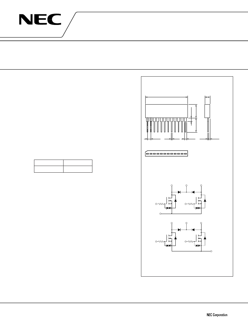
PACKAGE DIMENSIONS
(in millimeters)
CONNECTION DIAGRAM
2
3
4
D
6
D
5
D
2
R
G
D
1
R
G
Z
D
Z
D
1
6
5
9
10
11
D
8
D
7
D
4
R
G
D
3
R
G
Z
D
Z
D
8
7
12
D
1
to D
4
D
5
to D
8
Z
D
R
G
: Body Diode
: Surge Absorber
: Gate to Source Protection Diode
: Gate Input Resistance 330
TYP.
31.5 MAX.
4.2 MAX.
1 2 3 4 5 6 7 8 9 10 11 12
2.54 TYP.
0.7±0.1
1.4±0.1
0.5±0.1
1.4 TYP.
2
1
1
ELECTRODE CONNECTION
1, 5, 8, 12
2, 4, 9, 11
6, 7
3, 10
CATHODE
GATE
DRAIN, ANODE
SOURCE
相關(guān)PDF資料 |
PDF描述 |
|---|---|
| UPA1523 | P-CHANNEL POWER MOS FET ARRAY SWITCHING INDUSTRIAL USE |
| UPA1523B | CAP .01UF 50V UF(B) FILM SMD |
| UPA1523BH | CAP .1UF 50V PEN FILM 1913 5% |
| UPA1552 | N-CHANNEL POWER MOS FET ARRAY SWITCHING USE |
| UPA1552B | N-CHANNEL POWER MOS FET ARRAY SWITCHING USE |
相關(guān)代理商/技術(shù)參數(shù) |
參數(shù)描述 |
|---|---|
| UPA1500BH(AZ) | 制造商:Renesas Electronics Corporation 功能描述: |
| UPA1501 | 制造商:NEC 制造商全稱(chēng):NEC 功能描述:N - CHANNEL POWER MOS FET ARRAY SWITCHING TYPE |
| UPA1501H | 制造商:NEC 制造商全稱(chēng):NEC 功能描述:N - CHANNEL POWER MOS FET ARRAY SWITCHING TYPE |
| UPA1501H(AZ) | 制造商:Renesas Electronics Corporation 功能描述: |
| UPA1520B | 制造商:NEC 制造商全稱(chēng):NEC 功能描述:N-CHANNEL POWER MOS FET ARRAY SWITCHING USE |
發(fā)布緊急采購(gòu),3分鐘左右您將得到回復(fù)。