- 您現(xiàn)在的位置:買賣IC網(wǎng) > PDF目錄225366 > U4488B Quasi-Split Sound Circuit and AM Demodulator PDF資料下載
參數(shù)資料
| 型號(hào): | U4488B |
| 英文描述: | Quasi-Split Sound Circuit and AM Demodulator |
| 中文描述: | 準(zhǔn)分離聲音電路和AM解調(diào)器 |
| 文件頁(yè)數(shù): | 5/9頁(yè) |
| 文件大?。?/td> | 272K |
| 代理商: | U4488B |
U4488B
Preliminary Information
TELEFUNKEN Semiconductors
Rev. A2, 15-Jan-98
5 (9)
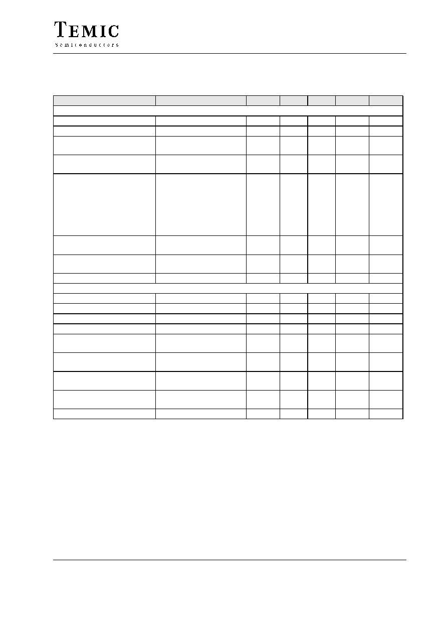
Electrical Characteristics (continued)
VS = + 5 V, Tamb = + 25°C; reference point Pin 13, unless otherwise specified
Parameters
Test Conditions / Pins
Symbol
Min.
Typ.
Max.
Unit
Intercarrier output
(Pin 12)
(see note 4)
DC output voltage
VDC
2
V
Output resistance
(See note 1)
Rout
200
W
Intercarrier output signal
vin = 10 mV
5.5 MHz output signal
Vout
100
150
mVrms
Intercarrier bandwidth
–1 dB
–3 dB
B
tbd
MHz
Weighted signal-to-noise ratio
(CCIR 468)
B/G mod. VIF signal:
vin = 10 mV;
FM dev. =
±27 kHz;
fmod = 1 kHz;
tested with U2860B;
Black screen: Channel 1/2
Color bar:
Channel 1/2
60/58
58/56
dB
Ripple rejection
Tested from Pin 14 to 12
(see note 1)
RR
35
dB
Allowable AC output peak
current
IAC
" 0.7
mA
Allowable DC output current
IDC
–2
mA
AF output – AM
(Pin 6)
(see note 5)
DC output voltage
VDC
2.2
V
Output resistance
(See note 1)
Rout
150
W
AF output signal
m = 54%
voAF
500
mVrms
AF bandwidth
–3 dB
B
tbd
kHz
Total harmonic distortion
m = 54%
fmod = 1 kHz, 12.5 kHz
THD
1
2
%
Weighted signal-to -oise ratio
(CCIR 468)
Reference: m = 54%;
fmod = 1 kHz
S/N
56
dB
Ripple rejection
Tested from Pin 14 to 6
(see note 1)
RR
28
dB
Allowable AC output peak
current
IAC
" 0.3
mA
Allowable DC output current
IDC
–1
mA
Notes
1.
This parameter is given as an application information and is not tested during production
2.
The oscillator drift is related to the picture carrier frequency, with external temperature compensated LC circuit
3.
Without external control voltage (Pin 7 open), the IC automatically operates in mode 1
4.
Picture carrier PC = 38.9 MHz; sound carrier SC1 = 33.4 MHz, SC2 = 33.16 MHz;
PC/SC1 =13 dB; PC/SC2 = 20 dB; PC unmodulated (equivalent to sync peak level)
5.
Sound carrier SC = 32.4 MHz, modulated with fmod = 1 kHz, m = 54%; vin = 10 mV
相關(guān)PDF資料 |
PDF描述 |
|---|---|
| U54-W-8 | GENERAL PURPOSE INDUCTOR |
| U54-W-7 | GENERAL PURPOSE INDUCTOR |
| U54-W-6 | GENERAL PURPOSE INDUCTOR |
| U54-W-69 | GENERAL PURPOSE INDUCTOR |
| U54-W-65 | GENERAL PURPOSE INDUCTOR |
相關(guān)代理商/技術(shù)參數(shù) |
參數(shù)描述 |
|---|---|
| U448B | 制造商:未知廠家 制造商全稱:未知廠家 功能描述:Telecommunication IC |
| U4490B | 制造商:未知廠家 制造商全稱:未知廠家 功能描述:TELEFUNK ELECTRONIC CREATIVE TECHNOLOGIEN U2200B-FP |
| U45 | 制造商:APEM 功能描述: |
| U4510011 | 制造商:LAPP OLFLEX 功能描述:Hook-up wire, HAR H07V-K, single core Black, 22 AWG, UL MTW, CSA, HAR, CE, 750V |
| U4520001 | 制造商:LAPP OLFLEX 功能描述:H07V-K 1.5 GREEN/YELLOW 16AWG HAR/CE-CX/1000 |
發(fā)布緊急采購(gòu),3分鐘左右您將得到回復(fù)。