- 您現(xiàn)在的位置:買賣IC網(wǎng) > PDF目錄225358 > TT150N18KOF 350 A, 1800 V, SCR PDF資料下載
參數(shù)資料
| 型號: | TT150N18KOF |
| 元件分類: | 晶閘管 |
| 英文描述: | 350 A, 1800 V, SCR |
| 文件頁數(shù): | 4/5頁 |
| 文件大小: | 197K |
| 代理商: | TT150N18KOF |
TT 150 N
Ptot
[W]
IRMS [A]
0
1200
TT 150 N/7
20
40
60
80
100
200
300
400
tA [°C]
200
400
600
800
1000
0.8
0.6
0.5
0.4
0.3
0.2
0.25
0.15
0.12
0.1
0.08
0.06
RthCA[°C/W]
0
500
0.05
0.04
0.03
Ptot
[W]
IRMS [A]
0
3000
TT 150 N/8
20
40
60
80
100
200
300
400
tA [°C]
1000
0.06
0.05
0.04
0.03
0.015
RthCA[°C/W]
0
500
0.1
1500
2000
2500
0.08
0.02
0.4
0.3
0.25
0.15
0.2
500
0.12
10
20
40
60 80 100
200
400 600 800
t [ms]
[kA]
IT(0V)M
1s
3,5
3,0
2,5
2,0
1,5
1,0
0,5
b
a
TT 150 N/9
104
102
100
2
3
4 5 6 7 8 101
2
3
4 5 6 7 8 102
-di/dt [A/s]
[As]
Qr
8
2
4
103
8
6
4
2
20 A
50 A
100 A
200 A
500 A
1000A
iTM=
TT 150 N/10
iG
0,1
0,2
0,5
1
2
5
10
20
30
[V]
vG
10
20 40
100 200 400
1
2
4
10
20
60
mA
A
a
b
c
d
60
600
6
40
100
TT 150 N/11
0,1
0,2
0,4
0,6
1
2
4
6
10
40
mA
A
20
60
102
4
6
103
tgd [s]
a
b
iG
TT 150 N/12
Bild / Fig. 12
Zündverzug/Gate controlled delay time tgd,
DIN 41787, ta = 1 s, tvj = 25°C.
a - uerster Verlauf/limiting characteristic
b - typischer Verlauf/typical charcteristic
10
20 40
100 200 400
1
2
4
10
20
60
600
6
40
100
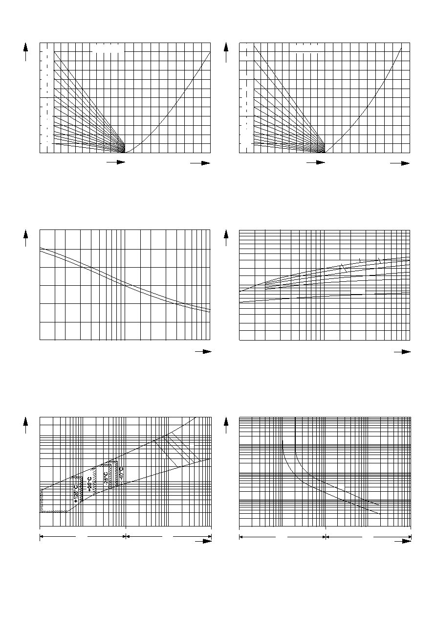
Bild / Fig. 10
Sperrverzgerungsladung / Recovery charge Qr = f(-di/dt)
tvj = tvjmax, vR ≤ 0,5 VRRM, vRM = 0,8 VRRM
Parameter: Durchlastrom / On-state current iTM
Bild / Fig. 9
Grenzstrom je Zweig IT(OV)M. Belastung aus Leerlauf, VRM = 0,8 VRRM
Maximum overload on- state current per arm IT(OV)M. Surge current under
no-load conditions, VR = 0,8 VRRM
a - tA = 35 °C, verstrkte Luftkühlung / forced cooling
b - tA = 45 °C, Luftselbstkühlung / natural cooling
Bild / Fig. 11
Steuercharakteristik mit Zündbereichen / Gate characteristic with triggering
areas, vG = f(iG), vD = 6 V
Parameter:
a
b
c
d
________________________________________________________
Steuerimpulsdauer / Pulse duration tg [ms] 10
1
0,5
0,1
________________________________________________________
Hchstzulssige Spitzensteuerleistung/
Maximum allowable peak gate power
[W]
40
80
100
150
________________________________________________________
Bild / Fig. 7
W1C - Einphasen-Wechselwegschaltung / Single-phase inverse parallel circuit
Hchstzulssiger Effektivstrom / Maximum ratet RMS current IRMS
Gesamtverlustleist. der Schaltung / Total power dissip. of the
circuit Ptot
Parameter: Wrmewiderstand zwischen Gehuse und Umgebung/
thermal resistance case to ambient RthCA
Bild / Fig. 8
W3C - Dreiphasen-Wechselwegschaltung / Three-phase inverse parallel circuit
Hchstzulssiger Effektivstrom je Phase / Maximum ratet RMS current per
phase IRMS
Gesamtverlustleist. der Schaltung / Total power dissip. of the circuit Ptot
Parameter: Wrmewiderstand zwischen Gehuse und Umgebung/
thermal resistance case to ambient RthCA
相關PDF資料 |
PDF描述 |
|---|---|
| TT150N18KOC | 350 A, 1800 V, SCR |
| TT162N10KOF | 260 A, 1000 V, SCR |
| TT162N06KOF | 260 A, 600 V, SCR |
| TT162N08KOF | 260 A, 800 V, SCR |
| TD162N06KOF | 260 A, 600 V, SCR |
相關代理商/技術參數(shù) |
參數(shù)描述 |
|---|---|
| TT150N19KOF | 制造商:n/a 功能描述:Power Module |
| TT150N20KOF | 功能描述:分立半導體模塊 2000V 350A DUAL RoHS:否 制造商:Infineon Technologies 產(chǎn)品:Thyristor Power Modules 類型:Phase Controls 安裝風格:Screw 封裝 / 箱體:DT61 封裝: |
| TT150N22KOF | 功能描述:分立半導體模塊 2200V 350A DUAL RoHS:否 制造商:Infineon Technologies 產(chǎn)品:Thyristor Power Modules 類型:Phase Controls 安裝風格:Screw 封裝 / 箱體:DT61 封裝: |
| TT150N23KOF | 制造商:n/a 功能描述:Power Module |
| TT150N24KOF | 功能描述:分立半導體模塊 2400V 350A DUAL RoHS:否 制造商:Infineon Technologies 產(chǎn)品:Thyristor Power Modules 類型:Phase Controls 安裝風格:Screw 封裝 / 箱體:DT61 封裝: |
發(fā)布緊急采購,3分鐘左右您將得到回復。