- 您現(xiàn)在的位置:買賣IC網(wǎng) > PDF目錄359758 > TSC87251G2D-L16IC 8/16-bit Microcontroller with Serial Communication Interfaces PDF資料下載
參數(shù)資料
| 型號(hào): | TSC87251G2D-L16IC |
| 元件分類: | 8位微控制器 |
| 英文描述: | 8/16-bit Microcontroller with Serial Communication Interfaces |
| 中文描述: | 16位產(chǎn)品微控制器的串行通信接口 |
| 文件頁數(shù): | 8/63頁 |
| 文件大小: | 878K |
| 代理商: | TSC87251G2D-L16IC |
第1頁第2頁第3頁第4頁第5頁第6頁第7頁當(dāng)前第8頁第9頁第10頁第11頁第12頁第13頁第14頁第15頁第16頁第17頁第18頁第19頁第20頁第21頁第22頁第23頁第24頁第25頁第26頁第27頁第28頁第29頁第30頁第31頁第32頁第33頁第34頁第35頁第36頁第37頁第38頁第39頁第40頁第41頁第42頁第43頁第44頁第45頁第46頁第47頁第48頁第49頁第50頁第51頁第52頁第53頁第54頁第55頁第56頁第57頁第58頁第59頁第60頁第61頁第62頁第63頁
8
Rev. A - May 7, 1999
TSC80251G2D
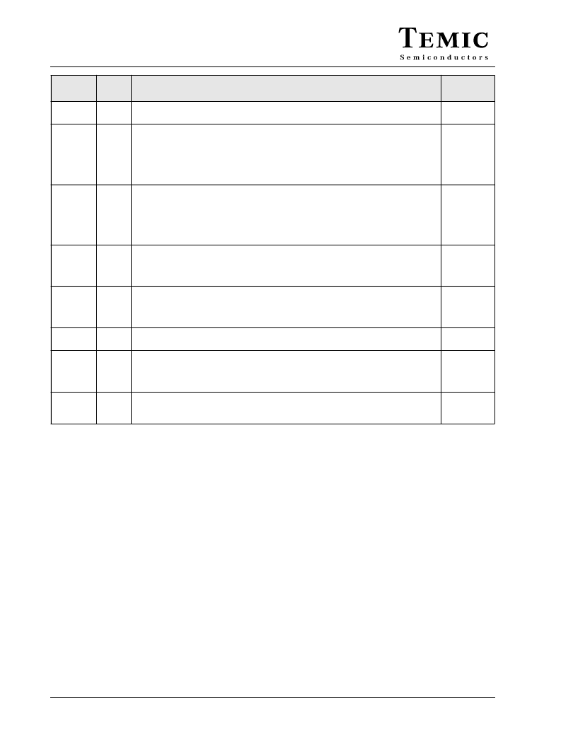
Note:
1. The description of A15:8/P2.7:0 and AD7:0/P0.7:0 are for the Non-Page mode chip configuration. If the chip is configured in Page mode
operation, port 0 carries the lower address bits (A7:0) while port 2 carries the upper address bits (A15:8) and the data (D7:0).
VSS
GND
Circuit Ground
Connect this pin to ground.
VSS1
GND
Secondary Ground 1
This ground is provided to reduce ground bounce and improve power supply bypassing.
Connection of this pin to ground is recommended. However, when using the TSC80251G2D
as a pin-for-pin replacement for a 8xC51 product, VSS1 can be unconnected without loss of
compatibility.
Not available on DIP package.
VSS2
GND
Secondary Ground 2
This ground is provided to reduce ground bounce and improve power supply bypassing.
Connection of this pin to ground is recommended. However, when using the TSC80251G2D
as a pin-for-pin replacement for a 8xC51 product, VSS2 can be unconnected without loss of
compatibility.
Not available on DIP package.
WAIT#
I
Real-time Synchronous Wait States Input
The real-time WAIT# input is enabled by setting RTWE bit in WCON (S:A7h). During bus
cycles, the external memory system can signal ‘system ready’ to the microcontroller in real
time by controlling the WAIT# input signal.
P1.6
WCLK
O
Wait Clock Output
The real-time WCLK output is enabled by setting RTWCE bit in WCON (S:A7h). When
enabled, the WCLK output produces a square wave signal with a period of one half the
oscillator frequency.
P1.7
WR#
O
Write
Write signal output to external memory.
P3.6
XTAL1
I
Input to the on-chip inverting oscillator amplifier
To use the internal oscillator, a crystal/resonator circuit is connected to this pin. If an external
oscillator is used, its output is connected to this pin. XTAL1 is the clock source for internal
timing.
XTAL2
O
Output of the on-chip inverting oscillator amplifier
To use the internal oscillator, a crystal/resonator circuit is connected to this pin. If an external
oscillator is used, leave XTAL2 unconnected.
Signal
Name
Type
Description
Alternate
Function
相關(guān)PDF資料 |
PDF描述 |
|---|---|
| TDA6501 | 5 V mixer/oscillator and synthesizer for PAL and NTSC standards |
| TDA6501TT | 5 V mixer/oscillator and synthesizer for PAL and NTSC standards |
| TSC87251G2D-24IJ | 8/16-bit Microcontroller with Serial Communication Interfaces |
| TSC251G1DXXX-24CED | IC CYCLONE III FPGA 55K 484 UBGA |
| TSC251G1DXXX-24IA | IC CYCLONE III FPGA 5K 144 EQFP |
相關(guān)代理商/技術(shù)參數(shù) |
參數(shù)描述 |
|---|---|
| TSC873CT A3 | 功能描述:兩極晶體管 - BJT NPN Silicon Planar Med Power Transistor RoHS:否 制造商:STMicroelectronics 配置: 晶體管極性:PNP 集電極—基極電壓 VCBO: 集電極—發(fā)射極最大電壓 VCEO:- 40 V 發(fā)射極 - 基極電壓 VEBO:- 6 V 集電極—射極飽和電壓: 最大直流電集電極電流: 增益帶寬產(chǎn)品fT: 直流集電極/Base Gain hfe Min:100 A 最大工作溫度: 安裝風(fēng)格:SMD/SMT 封裝 / 箱體:PowerFLAT 2 x 2 |
| TSC873CW RPG | 功能描述:兩極晶體管 - BJT NPN Silicon Planar Med Power Transistor RoHS:否 制造商:STMicroelectronics 配置: 晶體管極性:PNP 集電極—基極電壓 VCBO: 集電極—發(fā)射極最大電壓 VCEO:- 40 V 發(fā)射極 - 基極電壓 VEBO:- 6 V 集電極—射極飽和電壓: 最大直流電集電極電流: 增益帶寬產(chǎn)品fT: 直流集電極/Base Gain hfe Min:100 A 最大工作溫度: 安裝風(fēng)格:SMD/SMT 封裝 / 箱體:PowerFLAT 2 x 2 |
| TSC888AILT | 功能描述:電流靈敏放大器 Sense Amplifier 20 Gain RoHS:否 制造商:Texas Instruments 通道數(shù)量: 共模抑制比(最小值):110 dB 輸入補(bǔ)償電壓:80 uV 電源電壓-最大:5.5 V 電源電壓-最小:2.7 V 電源電流:350 uA 最大工作溫度:+ 125 C 最小工作溫度:- 40 C 安裝風(fēng)格:SMD/SMT 封裝 / 箱體:VQFN-16 封裝:Reel |
| TSC888BILT | 功能描述:電流靈敏放大器 Sense Amplifier 50 Gain RoHS:否 制造商:Texas Instruments 通道數(shù)量: 共模抑制比(最小值):110 dB 輸入補(bǔ)償電壓:80 uV 電源電壓-最大:5.5 V 電源電壓-最小:2.7 V 電源電流:350 uA 最大工作溫度:+ 125 C 最小工作溫度:- 40 C 安裝風(fēng)格:SMD/SMT 封裝 / 箱體:VQFN-16 封裝:Reel |
| TSC888CILT | 功能描述:電流靈敏放大器 Sense Amplifier 100 Gain RoHS:否 制造商:Texas Instruments 通道數(shù)量: 共模抑制比(最小值):110 dB 輸入補(bǔ)償電壓:80 uV 電源電壓-最大:5.5 V 電源電壓-最小:2.7 V 電源電流:350 uA 最大工作溫度:+ 125 C 最小工作溫度:- 40 C 安裝風(fēng)格:SMD/SMT 封裝 / 箱體:VQFN-16 封裝:Reel |
發(fā)布緊急采購(gòu),3分鐘左右您將得到回復(fù)。