- 您現(xiàn)在的位置:買賣IC網(wǎng) > PDF目錄382686 > TS5A3157YEPR (Texas Instruments, Inc.) 10-ohm SPDT ANALOG SWITCH PDF資料下載
參數(shù)資料
| 型號(hào): | TS5A3157YEPR |
| 廠商: | Texas Instruments, Inc. |
| 英文描述: | 10-ohm SPDT ANALOG SWITCH |
| 中文描述: | 10歐姆SPDT模擬開關(guān) |
| 文件頁(yè)數(shù): | 2/26頁(yè) |
| 文件大小: | 396K |
| 代理商: | TS5A3157YEPR |
第1頁(yè)當(dāng)前第2頁(yè)第3頁(yè)第4頁(yè)第5頁(yè)第6頁(yè)第7頁(yè)第8頁(yè)第9頁(yè)第10頁(yè)第11頁(yè)第12頁(yè)第13頁(yè)第14頁(yè)第15頁(yè)第16頁(yè)第17頁(yè)第18頁(yè)第19頁(yè)第20頁(yè)第21頁(yè)第22頁(yè)第23頁(yè)第24頁(yè)第25頁(yè)第26頁(yè)
www.ti.com
Absolute Minimum and Maximum Ratings
(1)(2)
over operating free-air temperature range (unless otherwise noted)
TS5A3157
10-
SPDT ANALOG SWITCH
SCDS199–JUNE 2005
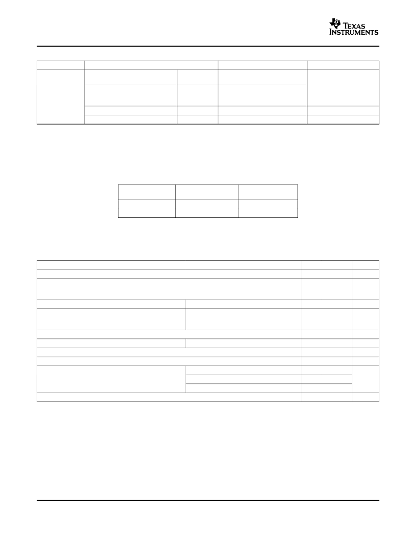
ORDERING INFORMATION
T
A
PACKAGE
(1)
ORDERABLE PART NUMBER
TOP-SIDE MARKING
(2)
NanoStar – WCSP (DSBGA)
0.23-mm Large Bump – YEP
NanoFree – WCSP (DSBGA)
0.23-mm Large Bump – YZP
(Pb-free)
SOT (SOT-23) – DBV
SOT (SC-70) – DCK
Tape and reel
TS5A3157YEPR
_ _ _JC_
Tape and reel
TS5A3157YZPR
–40
°
C to 85
°
C
Tape and reel
Tape and reel
TS5A3157DBVR
TS5A3157DCKR
JC5_
JC_
(1)
Package drawings, standard packing quantities, thermal data, symbolization, and PCB design guidelines are available at
www.ti.com/sc/package.
DBV/DCK: The actual top-side marking has one additional character that designates the assembly/test site.
YEP/YZP: The actual top-side marking has three preceding characters to denote year, month, and sequence code, and one following
character to designate the assembly/test site. Pin 1 identifier indicates solder-bump composition (1 = SnPb,
= Pb-free).
(2)
FUNCTION TABLE
NC TO COM,
COM TO NC
ON
OFF
NO TO COM,
COM TO NO
OFF
ON
IN
L
H
MIN
–0.5
MAX
6.5
UNIT
V
V
+
V
NO
V
NC
V
COM
I
K
I
NO
I
NC
I
COM
V
I
I
IK
I
+
I
GND
Supply voltage range
(3)
Analog voltage range
(3)(4)(5)
–0.5
V
+
+ 0.5
V
Analog port diode current
V
NC
, V
NO
, V
COM
< 0 or V
NO
, V
NC
, V
COM
> V
+
–50
50
mA
On-state switch current
V
NC
, V
NO
, V
COM
= 0 to V
+
–50
50
mA
Digital input voltage range
(3)(4)
Digital input clamp current
Continuous current through V
+
Continuous current through GND
–0.5
–50
–100
–100
6.5
V
V
I
< 0
mA
mA
mA
100
100
206
252
132
150
DBV package
DCK package
YEP/YZP package
θ
JA
Package thermal impedance
(6)
°C/W
T
stg
Storage temperature range
–65
°C
(1)
Stresses above these ratings may cause permanent damage. Exposure to absolute maximum conditions for extended periods may
degrade device reliability. These are stress ratings only, and functional operation of the device at these or any other conditions beyond
those specified is not implied.
The algebraic convention, whereby the most negative value is a minimum and the most positive value is a maximum.
All voltages are with respect to ground, unless otherwise specified.
The input and output voltage ratings may be exceeded if the input and output clamp-current ratings are observed.
This value is limited to 5.5 V maximum.
The package thermal impedance is calculated in accordance with JESD 51-7.
(2)
(3)
(4)
(5)
(6)
2
相關(guān)PDF資料 |
PDF描述 |
|---|---|
| TS61ID | Voltage-Feedback Operational Amplifier |
| TS7920 | |
| TS805C06 | SCHOTTKY DIODE |
| TS805C04 | SCHOTTKY BARRIER DIODE |
| TS8388BCG | A/D CONVERTER |
相關(guān)代理商/技術(shù)參數(shù) |
參數(shù)描述 |
|---|---|
| TS5A3157YZPR | 功能描述:模擬開關(guān) IC 10-Ohm SPST Analog Switch RoHS:否 制造商:Texas Instruments 開關(guān)數(shù)量:2 開關(guān)配置:SPDT 開啟電阻(最大值):0.1 Ohms 切換電壓(最大): 開啟時(shí)間(最大值): 關(guān)閉時(shí)間(最大值): 工作電源電壓:2.7 V to 4.5 V 最大工作溫度:+ 85 C 安裝風(fēng)格:SMD/SMT 封裝 / 箱體:DSBGA-16 |
| TS5A3159 | 制造商:TI 制造商全稱:Texas Instruments 功能描述:1-R SPDT ANALOG SWITCH |
| TS5A3159_09 | 制造商:TI 制造商全稱:Texas Instruments 功能描述:1-R SPDT ANALOG SWITCH |
| TS5A3159A | 制造商:TI 制造商全稱:Texas Instruments 功能描述:1-ohm SPDT ANALOG SWITCH 5-V/3.3-V SINGLE-CHANNEL 2:1 MULTIPLEXER/DEMULTIPLEXER |
| TS5A3159A_10 | 制造商:TI 制造商全稱:Texas Instruments 功能描述:1-Ω SPDT ANALOG SWITCH 5-V/3.3-V SINGLE-CHANNEL 2:1 MULTIPLEXER/DEMULTIPLEXER |
發(fā)布緊急采購(gòu),3分鐘左右您將得到回復(fù)。