- 您現(xiàn)在的位置:買賣IC網(wǎng) > PDF目錄382681 > TPS71H01Q (Texas Instruments, Inc.) LOW-DROPOUT VOLTAGE REGULATORS PDF資料下載
參數(shù)資料
| 型號(hào): | TPS71H01Q |
| 廠商: | Texas Instruments, Inc. |
| 元件分類: | 基準(zhǔn)電壓源/電流源 |
| 英文描述: | LOW-DROPOUT VOLTAGE REGULATORS |
| 中文描述: | 低壓差電壓調(diào)節(jié)器 |
| 文件頁數(shù): | 6/40頁 |
| 文件大?。?/td> | 634K |
| 代理商: | TPS71H01Q |
第1頁第2頁第3頁第4頁第5頁當(dāng)前第6頁第7頁第8頁第9頁第10頁第11頁第12頁第13頁第14頁第15頁第16頁第17頁第18頁第19頁第20頁第21頁第22頁第23頁第24頁第25頁第26頁第27頁第28頁第29頁第30頁第31頁第32頁第33頁第34頁第35頁第36頁第37頁第38頁第39頁第40頁
TPS71H01Q, TPS71H33Q, TPS71H48Q, TPS71H50Q
LOW-DROPOUT VOLTAGE REGULATORS
SLVS152B
–
NOVEMBER 1996
–
REVISED AUGUST 2002
6
POST OFFICE BOX 655303
DALLAS, TEXAS 75265
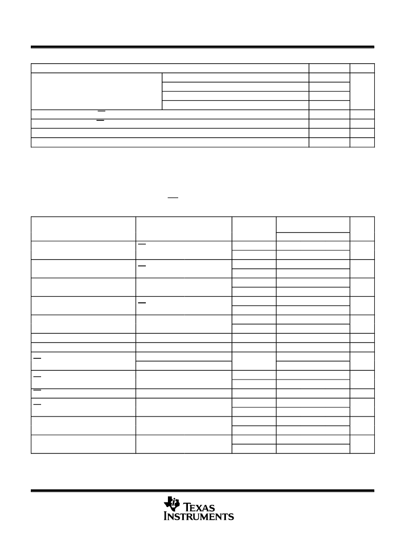
recommended operating conditions
MIN
2.5
MAX
UNIT
TPS71H01Q
10
Input voltage V
Input voltage, VI
TPS71H33Q
3.77
10
V
TPS71H48Q
5.2
10
TPS71H50Q
5.33
10
High-level input voltage at EN, VIH
Low-level input voltage at EN, VIL
Output current range, IO
Operating virtual junction temperature range, TJ
Minimum input voltage defined in the recommended operating conditions is the maximum specified output voltage plus dropout voltage at the
maximum specified load range. Since dropout voltage is a function of output current, the usable range can be extended for lighter loads. To
calculate the minimum input voltage for your maximum output current, use the following equation: VI(min) = VO(max) + VDO(max load)
Because the TPS71H01 is programmable, rDS(on) should be used to calculate VDO before applying the above equation. The equation for
calculating VDO from rDS(on) is given in Note 2 in the electrical characteristics table. The minimum value of 2.5 V is the absolute lower limit for
the recommended input voltage range for the TPS71H01.
2
V
0.5
V
0
500
mA
°
C
–
40
125
electrical characteristics at I
O
= 10 mA, EN = 0 V, C
O
= 4.7
μ
F/CSR
= 1
, SENSE/FB shorted to OUT
(unless otherwise noted)
PARAMETER
TEST CONDITIONS
§
TJ
TPS71H01Q, TPS71H33Q
TPS71H48Q, TPS71H50Q
MIN
TYP
285
UNIT
MAX
350
Ground current (active mode)
EN
0.5 V,
≤
0 mA
≤
IO
≤
500 mA
VI = VO + 1 V,
25
°
C
–
40
°
C to 125
°
C
25
°
C
–
40
°
C to 125
°
C
25
°
C
–
40
°
C to 125
°
C
25
°
C
–
40
°
C to 125
°
C
25
°
C
–
40
°
C to 125
°
C
–
40
°
C to 125
°
C
460
μ
A
Input current (standby mode)
EN = VI,
2 7 V
≤
≤
2.7 V
VI
10 V
0.5
2
μ
A
Output current limit
VO = 0,
VI = 10 V
1.2
2
A
2
Pass-element leakage current in standby
Pass element leakage current in standby
mode
EN = VI,
2 7 V
≤
≤
2.7 V
VI
10 V
0.5
1
μ
A
PG leakage current
Normal operation,
VPG = 10 V
0.02
0.5
0.5
μ
A
Output voltage temperature coefficient
61
75
ppm/
°
C
°
C
Thermal shutdown junction temperature
165
EN logic high (standby mode)
2.5 V
≤
VI
≤
6 V
6 V
≤
VI
≤
10 V
–
40
°
C to 125
°
C
2
V
2.7
EN logic low (active mode)
2 7 V
≤
≤
2.7 V
VI
10 V
25
°
C
0.5
V
–
40
°
C to 125
°
C
25
°
C
25
°
C
–
40
°
C to 125
°
C
25
°
C
–
40
°
C to 125
°
C
25
°
C
–
40
°
C to 125
°
C
0.5
EN hysteresis voltage
50
mV
EN input current
≤
≤
0 V
VI
10 V
–
0.5
0.5
–
0.5
0.5
μ
A
Minimum V for active pass element
Minimum VI for active pass element
2.05
2.5
V
2.5
Minimum VIfor valid PG
Minimum VI for valid PG
μ
A
IPG= 300
μ
A
IPG= 300
1.06
1.5
1.9
V
CSR (compensation series resistance) refers to the total series resistance, including the equivalent series resistance (ESR) of the capacitor, any
series resistance added externally, and PWB trace resistance to CO.
§
Pulse-testing techniques are used to maintain virtual junction temperature as close as possible to ambient temperature; thermal effects must
be taken into account separately.
相關(guān)PDF資料 |
PDF描述 |
|---|---|
| TPS71H01QPWP | LOW-DROPOUT VOLTAGE REGULATORS |
| TPS71H01QPWPLE | LOW-DROPOUT VOLTAGE REGULATORS |
| TPS71H33QPWPLE | TRANS PREBIASED PNP 200MW SOT23 |
| TPS71H33Q | LOW-DROPOUT VOLTAGE REGULATORS |
| TPS71H48Q | LOW-DROPOUT VOLTAGE REGULATORS |
相關(guān)代理商/技術(shù)參數(shù) |
參數(shù)描述 |
|---|---|
| TPS71H01QPWP | 制造商:Rochester Electronics LLC 功能描述:- Bulk |
| TPS71H01QPWPR | 功能描述:低壓差穩(wěn)壓器 - LDO LDO Reg RoHS:否 制造商:Texas Instruments 最大輸入電壓:36 V 輸出電壓:1.4 V to 20.5 V 回動(dòng)電壓(最大值):307 mV 輸出電流:1 A 負(fù)載調(diào)節(jié):0.3 % 輸出端數(shù)量: 輸出類型:Fixed 最大工作溫度:+ 125 C 安裝風(fēng)格:SMD/SMT 封裝 / 箱體:VQFN-20 |
| TPS71H01QPWPRG4 | 功能描述:低壓差穩(wěn)壓器 - LDO LDO Reg RoHS:否 制造商:Texas Instruments 最大輸入電壓:36 V 輸出電壓:1.4 V to 20.5 V 回動(dòng)電壓(最大值):307 mV 輸出電流:1 A 負(fù)載調(diào)節(jié):0.3 % 輸出端數(shù)量: 輸出類型:Fixed 最大工作溫度:+ 125 C 安裝風(fēng)格:SMD/SMT 封裝 / 箱體:VQFN-20 |
| TPS71H33QPWP | 制造商:Rochester Electronics LLC 功能描述:- Bulk 制造商:Texas Instruments 功能描述: |
| TPS71H33QPWPR | 功能描述:低壓差穩(wěn)壓器 - LDO LDO Reg RoHS:否 制造商:Texas Instruments 最大輸入電壓:36 V 輸出電壓:1.4 V to 20.5 V 回動(dòng)電壓(最大值):307 mV 輸出電流:1 A 負(fù)載調(diào)節(jié):0.3 % 輸出端數(shù)量: 輸出類型:Fixed 最大工作溫度:+ 125 C 安裝風(fēng)格:SMD/SMT 封裝 / 箱體:VQFN-20 |
發(fā)布緊急采購,3分鐘左右您將得到回復(fù)。