- 您現(xiàn)在的位置:買賣IC網(wǎng) > PDF目錄382679 > TPS54614PWP Analog IC PDF資料下載
參數(shù)資料
| 型號: | TPS54614PWP |
| 英文描述: | Analog IC |
| 中文描述: | 模擬IC |
| 文件頁數(shù): | 7/16頁 |
| 文件大小: | 260K |
| 代理商: | TPS54614PWP |
TPS54611, TPS54612, TPS54613
TPS54614, TPS54615, TPS54616
SLVS400A
–
AUGUST 2001
–
REVISED JANUARY 2002
7
www.ti.com
detailed description
under voltage lock out (UVLO)
The TPS5461x incorporates an under voltage lockout circuit to keep the device disabled when the input voltage
(VIN) is insufficient. During power up, internal circuits are held inactive until VIN exceeds the nominal UVLO
threshold voltage of 2.95 V. Once the UVLO start threshold is reached, device start-up begins. The device
operates until VIN falls below the nominal UVLO stop threshold of 2.8 V. Hysteresis in the UVLO comparator,
and a 2.5-
μ
s rising and falling edge deglitch circuit reduce the likelihood of shutting the device down due to noise
on VIN.
slow-start/enable (SS/ENA)
The slow-start/enable pin provides two functions. First, the pin acts as an enable (shutdown) control by keeping
the device turned off until the voltage exceeds the start threshold voltage of approximately 1.2 V. When SS/ENA
exceeds the enable threshold, device start up begins. The reference voltage fed to the error amplifier is linearly
ramped up from 0 V to 0.891 V in 3.35 ms. Similarly, the converter output voltage reaches regulation in
approximately 3.35 ms. Voltage hysteresis and a 2.5-
μ
s falling edge deglitch circuit reduce the likelihood of
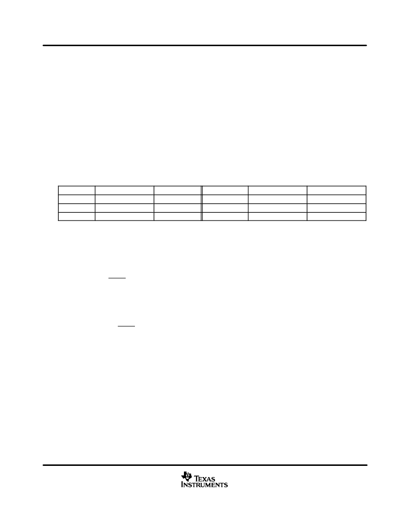
triggering the enable due to noise. Refer to the following table for start up times for each device
DEVICE
OUTPUT VOLTAGE
SLOW-START
DEVICE
OUTPUT VOLTAGE
SLOW-START
TPS54611
0.9 V
3.3 ms
TPS54614
1.8 V
3.3 ms
TPS54612
1.2 V
4.5 ms
TPS54615
2.5 V
4.7 ms
TPS54613
1.5 V
5.6 ms
TPS54616
3.3 V
6.1 ms
The second function of the SS/ENA pin provides an external means for extending the slow-start time with a
ceramic capacitor connected between SS/ENA and AGND. Adding a capacitor to the SS/ENA pin has two
effects on start-up. First, a delay occurs between release of the SS/ENA pin and start-up of the output. The delay
is proportional to the slow-start capacitor value and lasts until the SS/ENA pin reaches the enable threshold.
The start-up delay is approximately:
td
C(SS)
1.2 V
5
A
Second, as the output becomes active, a brief ramp up at the internal slow-start rate may be observed before
the externally set slow-start rate takes control and the output rises at a rate proportional to the slow-start
capacitor. The slow-start time set by the capacitor is approximately:
t(SS)
C(SS)
0.7 V
5
A
The actual slow-start time is likely to be less than the above approximation due to the brief ramp up at the internal
rate.
VBIAS regulator
The VBIAS regulator provides internal analog and digital blocks with a stable supply voltage over variations in
junction temperature and input voltage. A high quality, low-ESR, ceramic bypass capacitor is required on the
VBIAS pin. X7R or X5R grade dielectrics are recommended because their values are more stable over
temperature. The bypass capacitor should be placed close to the VBIAS pin and returned to AGND.
External loading on VBIAS is allowed, with the caution that internal circuits require a minimum VBIAS of 2.7 V,
and external loads on VBIAS with ac or digital switching noise may degrade performance. The VBIAS pin may
be useful as a reference voltage for external circuits.
voltage reference
The voltage reference system produces a precise, temperature-stable voltage from a bandgap circuit. A scaling
amplifier and DAC are then used to produce the reference voltages for each of the fixed output devices.
(1)
(2)
相關(guān)PDF資料 |
PDF描述 |
|---|---|
| TPS54614PWPR | Analog IC |
| TPS54615PWP | Analog IC |
| TPS54615PWPR | Analog IC |
| TPS54616PWP | Analog IC |
| TPS54616PWPR | Analog IC |
相關(guān)代理商/技術(shù)參數(shù) |
參數(shù)描述 |
|---|---|
| TPS54614PWP | 制造商:Texas Instruments 功能描述:BUCK PWM REG FET 6A SMD 54614 |
| TPS54614PWPG4 | 功能描述:直流/直流開關(guān)調(diào)節(jié)器 Lo-In Voltage 6A Sync Buck Converter RoHS:否 制造商:International Rectifier 最大輸入電壓:21 V 開關(guān)頻率:1.5 MHz 輸出電壓:0.5 V to 0.86 V 輸出電流:4 A 輸出端數(shù)量: 最大工作溫度: 安裝風(fēng)格:SMD/SMT 封裝 / 箱體:PQFN 4 x 5 |
| TPS54614PWPR | 功能描述:直流/直流開關(guān)調(diào)節(jié)器 Lo-In Voltage 6A Sync Buck Converter RoHS:否 制造商:International Rectifier 最大輸入電壓:21 V 開關(guān)頻率:1.5 MHz 輸出電壓:0.5 V to 0.86 V 輸出電流:4 A 輸出端數(shù)量: 最大工作溫度: 安裝風(fēng)格:SMD/SMT 封裝 / 箱體:PQFN 4 x 5 |
| TPS54614PWPRG4 | 功能描述:直流/直流開關(guān)調(diào)節(jié)器 Lo-In Voltage 6A Sync Buck Converter RoHS:否 制造商:International Rectifier 最大輸入電壓:21 V 開關(guān)頻率:1.5 MHz 輸出電壓:0.5 V to 0.86 V 輸出電流:4 A 輸出端數(shù)量: 最大工作溫度: 安裝風(fēng)格:SMD/SMT 封裝 / 箱體:PQFN 4 x 5 |
| TPS54614-Q1 | 制造商:TI 制造商全稱:Texas Instruments 功能描述:3-V TO 6-V INPUT, 6-A OUTPUT SYNCHRONOUS BUCK PWM SWITCHER WITH INTEGRATED FETs(SWIFT) |
發(fā)布緊急采購,3分鐘左右您將得到回復(fù)。