- 您現(xiàn)在的位置:買賣IC網(wǎng) > PDF目錄225340 > TPS5410MDREP (TEXAS INSTRUMENTS INC) 4.6 A SWITCHING REGULATOR, 600 kHz SWITCHING FREQ-MAX, PDSO8 PDF資料下載
參數(shù)資料
| 型號: | TPS5410MDREP |
| 廠商: | TEXAS INSTRUMENTS INC |
| 元件分類: | 穩(wěn)壓器 |
| 英文描述: | 4.6 A SWITCHING REGULATOR, 600 kHz SWITCHING FREQ-MAX, PDSO8 |
| 封裝: | GREEN, PLASTIC, SOIC-8 |
| 文件頁數(shù): | 6/25頁 |
| 文件大小: | 759K |
| 代理商: | TPS5410MDREP |
R2 +
R1
1.221
V
OUT *
1.221
GND
VSNS
VIN
NC
ENA
BOOT
PH
VIN
U1
TPS5410D
5V
7V
36V
-
C1
4.7 F
m
C4
47 F
m
(Note A)
C2
0.01 F
m
L1
68 H
m
R2
3.24kW
D1
B340A
7
1
5
8
2
4
3
6
VOUT
ENA
R1
10kW
R3
1.78kW
C6
2700pF
C5
150pF
C7
0.056 F
m
C3
47 F
m
(Note A)
C
(MIN)
O
1
2
(2
x7000)xL
p
O
SLVS910 – SEPTEMBER 2009 ......................................................................................................................................................................................... www.ti.com
(12)
For any TPS5410 design, start with an R1 value of 10 k
. R2 is then 1.13 k.
Boot Capacitor
The boot capacitor should be 0.01
μF.
Catch Diode
The TPS5410 is designed to operate using an external catch diode between PH and GND. The selected diode
must meet the absolute maximum ratings for the application: Reverse voltage must be higher than the maximum
voltage at the PH pin, which is VINMAX + 0.5 V. Peak current must be greater than IOUTMAX plus on half the
peak-to-peak inductor current. Forward voltage drop should be small for higher efficiencies. It is important to note
that the catch diode conduction time is typically longer than the high-side FET on time; therefore, the diode
parameters improve the overall efficiency. Additionally, check that the device chosen is capable of dissipating the
power losses. For this design, a Diodes, Inc. B340A is chosen, with a reverse voltage of 40 V, forward current of
3 A, and a forward voltage drop of 0.5 V.
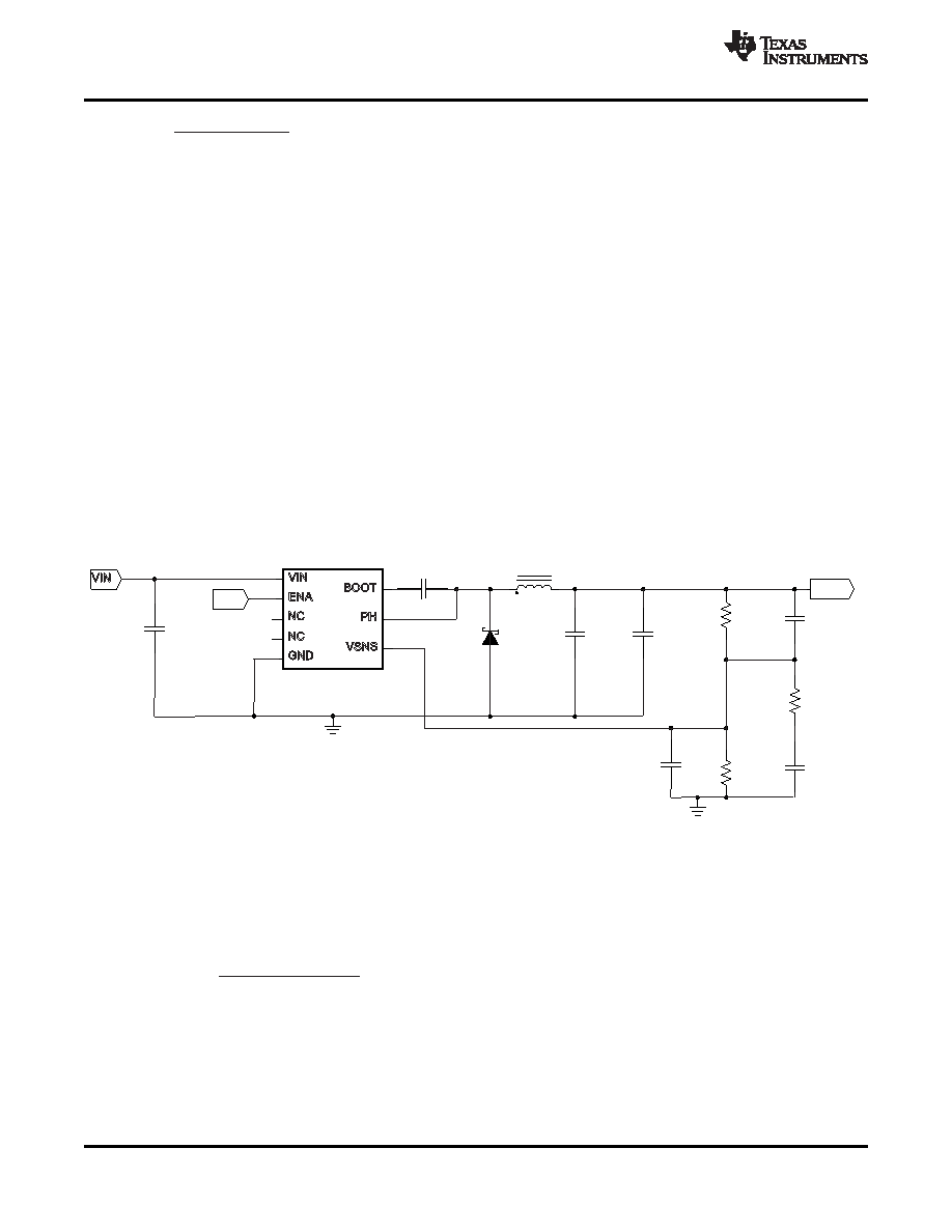
Additional Circuits
Figure 12 shows an application circuit using all ceramic capacitors for the input and output filters. The design
procedure is similar to those given for the design example, except for the selection of the output filter capacitor
values and the design of the additional compensation components required to stabilize the circuit.
A.
C3, C4 = Ceramic TDKC4532X5R1A476MT
Figure 12. 7-V — 36-V Input to 5-V Output Application Circuit with Ceramic Capacitors
Output Filter Capacitor Selection
When using ceramic output filer capacitors, the recommended LC resonant frequency should be no more than 7
kHz. Since the output inductor is already selected at 68
μH, this limits the minimum output capacitor value to:
(13)
The minimum capacitor value is calculated to be 7.6
μF. For this circuit a larger value of capacitor will yield better
transient response. Two output capacitors are used for C3 and C4 with a value of 47 uF each. It is important to
note that the actual capacitance of ceramic capacitors decreases with applied voltage. In this case the effective
value used for the calculations is approximately 70 % of the rated value or 70
μF.
14
Copyright 2009, Texas Instruments Incorporated
Product Folder Link(s): TPS5410-EP
相關(guān)PDF資料 |
PDF描述 |
|---|---|
| TPS54429ERSAT | 0.01 A SWITCHING REGULATOR, PQCC16 |
| TPS60201DGSRG4 | SWITCHED CAPACITOR REGULATOR, 400 kHz SWITCHING FREQ-MAX, PDSO10 |
| TPS62000 | "Adjustable |
| TPS65166RHAR | SPECIALTY ANALOG CIRCUIT, PQCC40 |
| TPS65270RGET | DUAL SWITCHING CONTROLLER, 1400 kHz SWITCHING FREQ-MAX, PQCC24 |
相關(guān)代理商/技術(shù)參數(shù) |
參數(shù)描述 |
|---|---|
| TPS5410-Q1 | 制造商:TI 制造商全稱:Texas Instruments 功能描述:1-A, WIDE INPUT RANGE, STEP-DOWN SWIFTa?¢ CONVERTER |
| TPS5410QDRQ1 | 功能描述:直流/直流開關(guān)調(diào)節(jié)器 AC 5.5-36V,1A,500kHz RoHS:否 制造商:International Rectifier 最大輸入電壓:21 V 開關(guān)頻率:1.5 MHz 輸出電壓:0.5 V to 0.86 V 輸出電流:4 A 輸出端數(shù)量: 最大工作溫度: 安裝風(fēng)格:SMD/SMT 封裝 / 箱體:PQFN 4 x 5 |
| TPS54110 | 制造商:TI 制造商全稱:Texas Instruments 功能描述:SWIFT Converter Product Portfolio |
| TPS54110EVM-044 | 功能描述:電源管理IC開發(fā)工具 3-6Vin DC/DC Conv RoHS:否 制造商:Maxim Integrated 產(chǎn)品:Evaluation Kits 類型:Battery Management 工具用于評估:MAX17710GB 輸入電壓: 輸出電壓:1.8 V |
| TPS54110EVM-044 | 制造商:Texas Instruments 功能描述:EVAL BOARD, TPS54110 ADJ 1.5A STEP-DOWN |
發(fā)布緊急采購,3分鐘左右您將得到回復(fù)。