- 您現(xiàn)在的位置:買賣IC網(wǎng) > PDF目錄385945 > TPS2022P (Texas Instruments, Inc.) POWER-DISTRIBUTION SWITCHES PDF資料下載
參數(shù)資料
| 型號(hào): | TPS2022P |
| 廠商: | Texas Instruments, Inc. |
| 英文描述: | POWER-DISTRIBUTION SWITCHES |
| 中文描述: | 配電開(kāi)關(guān) |
| 文件頁(yè)數(shù): | 19/23頁(yè) |
| 文件大?。?/td> | 377K |
| 代理商: | TPS2022P |
第1頁(yè)第2頁(yè)第3頁(yè)第4頁(yè)第5頁(yè)第6頁(yè)第7頁(yè)第8頁(yè)第9頁(yè)第10頁(yè)第11頁(yè)第12頁(yè)第13頁(yè)第14頁(yè)第15頁(yè)第16頁(yè)第17頁(yè)第18頁(yè)當(dāng)前第19頁(yè)第20頁(yè)第21頁(yè)第22頁(yè)第23頁(yè)
TPS2020, TPS2021, TPS2022, TPS2023, TPS2024
POWER-DISTRIBUTION SWITCHES
SLVS175A – DECEMBER 1998 – REVISED NOVEMBER 1999
19
POST OFFICE BOX 655303
DALLAS, TEXAS 75265
APPLICATION INFORMATION
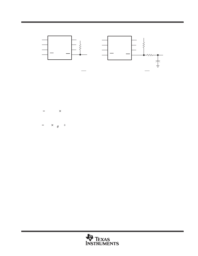
GND
IN
IN
EN
OUT
OC
OUT
OUT
TPS202x
GND
IN
IN
EN
OUT
OC
OUT
OUT
TPS202x
Rpullup
V+
Rfilter
Rpullup
Cfilter
V+
Figure 39. Typical Circuit for OC Pin and RC Filter for Damping Inrush OC Responses
power dissipation and junction temperature
The low on-resistance on the n-channel MOSFET allows small surface-mount packages, such as SOIC, to pass
large currents. The thermal resistances of these packages are high compared to those of power packages; it
is good design practice to check power dissipation and junction temperature. The first step is to find r
DS(on)
at
the input voltage and operating temperature. As an initial estimate, use the highest operating ambient
temperature of interest and read r
DS(on)
from Figures 33–36. Next, calculate the power dissipation using:
I2
PD
rDS(on)
Finally, calculate the junction temperature:
TJ
PD
RJA
TA
Where:
T
A
= Ambient Temperature
°
C
R
θ
JA
= Thermal resistance SOIC = 172
°
C/W, PDIP = 106
°
C/W
Compare the calculated junction temperature with the initial estimate. If they do not agree within a few degrees,
repeat the calculation, using the calculated value as the new estimate. Two or three iterations are generally
sufficient to get an acceptable answer.
thermal protection
Thermal protection prevents damage to the IC when heavy-overload or short-circuit faults are present for
extended periods of time. The faults force the TPS202x into constant current mode, which causes the voltage
across the high-side switch to increase; under short-circuit conditions, the voltage across the switch is equal
to the input voltage. The increased dissipation causes the junction temperature to rise to high levels. The
protection circuit senses the junction temperature of the switch and shuts it off. Hysteresis is built into the thermal
sense circuit, and after the device has cooled approximately 20 degrees, the switch turns back on. The switch
continues to cycle in this manner until the load fault or input power is removed.
undervoltage lockout (UVLO)
An undervoltage lockout ensures that the power switch is in the off state at powerup. Whenever the input voltage
falls below approximately 2 V, the power switch will be quickly turned off. This facilitates the design of
hot-insertion systems where it is not possible to turn off the power switch before input power is removed. The
UVLO will also keep the switch from being turned on until the power supply has reached at least 2 V, even if
the switch is enabled. Upon reinsertion, the power switch will be turned on, with a controlled rise time to reduce
EMI and voltage overshoots.
相關(guān)PDF資料 |
PDF描述 |
|---|---|
| TPS202X | USB POWER DISTRIBUTION |
| TPS204X | USB POWER DISTRIBUTION |
| TPS203X | USB POWER DISTRIBUTION |
| TPS2032P | POWER-DISTRIBUTION SWITCHES |
| TPS2033P | POWER-DISTRIBUTION SWITCHES |
相關(guān)代理商/技術(shù)參數(shù) |
參數(shù)描述 |
|---|---|
| TPS2022PE4 | 功能描述:電源開(kāi)關(guān) IC - USB 1.1A 2.7-5.5V Sngl Hi-Side MOSFET RoHS:否 制造商:Micrel 電源電壓-最小:2.7 V 電源電壓-最大:5.5 V 最大工作溫度:+ 85 C 最小工作溫度:- 40 C 封裝 / 箱體:SOIC-8 封裝:Tube |
| TPS2022-Q1 | 制造商:TI 制造商全稱:Texas Instruments 功能描述:POWER-DISTRIBUTION SWITCHES |
| TPS2023 | 制造商:TI 制造商全稱:Texas Instruments 功能描述:POWER-DISTRIBUTION SWITCHES |
| TPS2023D | 功能描述:電源開(kāi)關(guān) IC - USB 1.65A 2.7-5.5V Sngl Hi-Side MOSFET RoHS:否 制造商:Micrel 電源電壓-最小:2.7 V 電源電壓-最大:5.5 V 最大工作溫度:+ 85 C 最小工作溫度:- 40 C 封裝 / 箱體:SOIC-8 封裝:Tube |
| TPS2023D | 制造商:Texas Instruments 功能描述:IC 2.2A POWER DIST SWITCH 8-SOIC 制造商:Texas Instruments 功能描述:IC, 2.2A POWER DIST SWITCH 8-SOIC 制造商:Texas Instruments 功能描述:IC, 2.2A POWER DIST SWITCH 8-SOIC; Primary Input Voltage:5.5V; No. of Outputs:1; Output Current:1.5A; Voltage Regulator Case Style:SOIC; No. of Pins:8; Operating Temperature Min:-40C; Operating Temperature Max:85C; SVHC:No SVHC ;RoHS Compliant: Yes |
發(fā)布緊急采購(gòu),3分鐘左右您將得到回復(fù)。