- 您現(xiàn)在的位置:買賣IC網(wǎng) > PDF目錄98271 > TPA2036D1YZFT (TEXAS INSTRUMENTS INC) 2.5 W, 1 CHANNEL, AUDIO AMPLIFIER, PBGA9 PDF資料下載
參數(shù)資料
| 型號: | TPA2036D1YZFT |
| 廠商: | TEXAS INSTRUMENTS INC |
| 元件分類: | 音頻/視頻放大 |
| 英文描述: | 2.5 W, 1 CHANNEL, AUDIO AMPLIFIER, PBGA9 |
| 封裝: | 1.45 X 1.45 MM, LEAD FREE, BGA-9 |
| 文件頁數(shù): | 8/24頁 |
| 文件大?。?/td> | 743K |
| 代理商: | TPA2036D1YZFT |
Component Location
Trace Width
SLOS589 – OCTOBER 2008.............................................................................................................................................................................................. www.ti.com
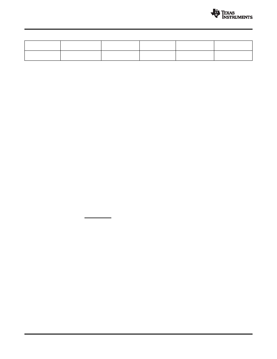
Table 2. Land Pattern Dimensions
SOLDER PAD
SOLDER MASK
COPPER
STENCIL
COPPER PAD
DEFINITIONS
OPENING
THICKNESS
OPENING
THICKNESS
Nonsolder mask
275
m
375
m
1 oz max (32
m)
275
m x 275 m Sq.
125
m thick
defined (NSMD)
(+0.0, –25
m)
(+0.0, –25
m)
(rounded corners)
NOTES:
1. Circuit traces from NSMD defined PWB lands should be 75
m to 100 m wide in the exposed area inside
the solder mask opening. Wider trace widths reduce device stand off and impact reliability.
2. Recommend solder paste is Type 3 or Type 4.
3. Best reliability results are achieved when the PWB laminate glass transition temperature is above the
operating the range of the intended application.
4. For a PWB using a Ni/Au surface finish, the gold thickness should be less 0.5
m to avoid a reduction in
thermal fatigue performance.
5. Solder mask thickness should be less than 20
m on top of the copper circuit pattern.
6. Best solder stencil performance is achieved using laser cut stencils with electro polishing. Use of chemically
etched stencils results in inferior solder paste volume control.
7. Trace routing away from WCSP device should be balanced in X and Y directions to avoid unintentional
component movement due to solder wetting forces.
Place all the external components very close to the TPA2036D1. The input resistors need to be very close to the
TPA2036D1 input pins so noise does not couple on the high impedance nodes between the input resistors and
the input amplifier of the TPA2036D1. Placing the decoupling capacitor, CS, close to the TPA2036D1 is
important for the efficiency of the class-D amplifier. Any resistance or inductance in the trace between the device
and the capacitor can cause a loss in efficiency.
Recommended trace width at the solder balls is 75
m to 100 m to prevent solder wicking onto wider PCB
traces. Figure 34 shows the layout of the TPA2036D1 evaluation module (EVM).
For high current pins (VDD, GND VO+, and VO–) of the TPA2036D1, use 100-m trace widths at the solder balls
and at least 500-
m PCB traces to ensure proper performance and output power for the device.
For input pins (IN–, IN+, and SHUTDOWN) of the TPA2036D1, use 75-
m to 100-m trace widths at the solder
balls. IN– and IN+ pins need to run side-by-side to maximize common-mode noise cancellation. Placing input
resistors, RIN, as close to the TPA2036D1 as possible is recommended.
16
Copyright 2008, Texas Instruments Incorporated
Product Folder Link(s): TPA2036D1
相關(guān)PDF資料 |
PDF描述 |
|---|---|
| TPA2036D1YZF | 2.5 W, 1 CHANNEL, AUDIO AMPLIFIER, PBGA9 |
| TPA2037D1YFFR | 3.24 W, 1 CHANNEL, AUDIO AMPLIFIER, BGA9 |
| TPA2037D1YFFT | 3.24 W, 1 CHANNEL, AUDIO AMPLIFIER, BGA9 |
| TPA2039D1YFFR | 3.24 W, 1 CHANNEL, AUDIO AMPLIFIER, BGA9 |
| TPA2039D1YFFT | 3.24 W, 1 CHANNEL, AUDIO AMPLIFIER, BGA9 |
相關(guān)代理商/技術(shù)參數(shù) |
參數(shù)描述 |
|---|---|
| TPA2036D1YZFT | 制造商:Texas Instruments 功能描述:2.5-W Mono Class-D Audio Power Amplifier |
| TPA2037D1 | 制造商:TI 制造商全稱:Texas Instruments 功能描述:3.2W Mono Class-D Audio Power Amplifier With 6-dB Gain and Auto Short-Circuit Recovery |
| TPA2037D1YFFEVM | 功能描述:音頻 IC 開發(fā)工具 TPA2037D1YFFEVM Eval Mod RoHS:否 制造商:Texas Instruments 產(chǎn)品:Evaluation Kits 類型:Audio Amplifiers 工具用于評估:TAS5614L 工作電源電壓:12 V to 38 V |
| TPA2037D1YFFR | 功能描述:音頻放大器 Fixed Gain 3.2 W Mono Class-D RoHS:否 制造商:STMicroelectronics 產(chǎn)品:General Purpose Audio Amplifiers 輸出類型:Digital 輸出功率: THD + 噪聲: 工作電源電壓:3.3 V 電源電流: 最大功率耗散: 最大工作溫度: 安裝風(fēng)格:SMD/SMT 封裝 / 箱體:TQFP-64 封裝:Reel |
| TPA2037D1YFFT | 功能描述:音頻放大器 Fixed Gain 3.2 W Mono Class-D RoHS:否 制造商:STMicroelectronics 產(chǎn)品:General Purpose Audio Amplifiers 輸出類型:Digital 輸出功率: THD + 噪聲: 工作電源電壓:3.3 V 電源電流: 最大功率耗散: 最大工作溫度: 安裝風(fēng)格:SMD/SMT 封裝 / 箱體:TQFP-64 封裝:Reel |
發(fā)布緊急采購,3分鐘左右您將得到回復(fù)。