- 您現(xiàn)在的位置:買賣IC網(wǎng) > PDF目錄384025 > TPA2012D2YZH (Texas Instruments, Inc.) 2.1 W/CH STEREO FILTER-FREE CLASS-D AUDIO POWER AMPLIFIER PDF資料下載
參數(shù)資料
| 型號(hào): | TPA2012D2YZH |
| 廠商: | Texas Instruments, Inc. |
| 英文描述: | 2.1 W/CH STEREO FILTER-FREE CLASS-D AUDIO POWER AMPLIFIER |
| 中文描述: | 2.1瓦/甲烷立體聲無(wú)濾波器D類音頻功率放大器 |
| 文件頁(yè)數(shù): | 14/20頁(yè) |
| 文件大小: | 722K |
| 代理商: | TPA2012D2YZH |
第1頁(yè)第2頁(yè)第3頁(yè)第4頁(yè)第5頁(yè)第6頁(yè)第7頁(yè)第8頁(yè)第9頁(yè)第10頁(yè)第11頁(yè)第12頁(yè)第13頁(yè)當(dāng)前第14頁(yè)第15頁(yè)第16頁(yè)第17頁(yè)第18頁(yè)第19頁(yè)第20頁(yè)
www.ti.com
Trace Width
Recommended trace width at the solder balls is 75
μ
m to 100
μ
m to prevent solder wicking onto wider PCB
traces.
For high current pins (PV
, PGND, and audio output pins) of the TPA2012D2, use 100-
μ
m trace widths at the
solder balls and at least 500-
μ
m PCB traces to ensure proper performance and output power for the device.
For the remaining signals of the TPA2012D2, use 75-
μ
m to 100-
μ
m trace widths at the solder balls. The audio
input pins (INR+/- and INL+/-) must run side-by-side to maximize common-mode noise cancellation.
EFFICIENCY AND THERMAL INFORMATION
The maximum ambient temperature depends on the heat-sinking ability of the PCB system. The derating factor
for the packages are shown in the dissipation rating table. Converting this to
θ
JA
for the QFN package:
JA
1
Derating Factor
1
0.041
24
°
C W
(3)
TAMax
TJMax
JAPDmax
150
24 (1.5)
114
°
C
(4)
OPERATION WITH DACs AND CODECs
In using Class-D amplifiers with CODECs and DACs, sometimes there is an increase in the output noise floor
from the audio amplifier. This occurs when mixing of the output frequencies of the CODEC/DAC mix with the
switching frequencies of the audio amplifier input stage. The noise increase can be solved by placing a low-pass
filter between the CODEC/DAC and audio amplifier. This filters off the high frequencies that cause the problem
and allow proper performance. See
Figure 33
for the block diagram.
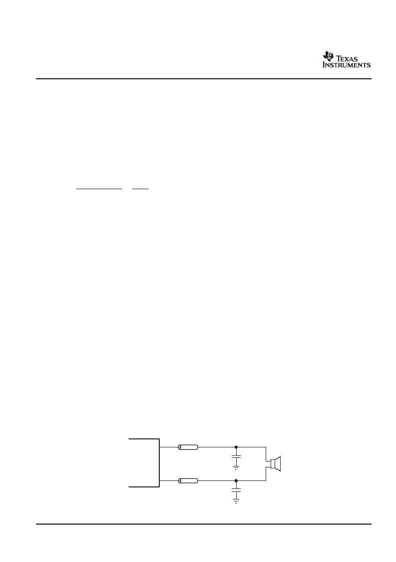
FILTER FREE OPERATION AND FERRITE BEAD FILTERS
1 nF
Ferrite
Chip Bead
OUTP
OUTN
Ferrite
Chip Bead
1 nF
TPA2012D2
SLOS438C–DECEMBER 2004–REVISED MARCH 2007
Given
θ
JA
of 24
°
C/W, the maximum allowable junction temperature of 150
°
C, and the maximum internal
dissipation of 1.5W (0.75 W per channel) for 2.1 W per channel, 4-
load, 5-V supply, from
Figure 25
, the
maximum ambient temperature can be calculated with the following equation.
Equation 4
shows that the calculated maximum ambient temperature is 114
°
C at maximum power dissipation
with a 5-V supply and 4-
a load. The TPA2012D2 is designed with thermal protection that turns the device off
when the junction temperature surpasses 150
°
C to prevent damage to the IC. Also, using speakers more
resistive than 4-
dramatically increases the thermal performance by reducing the output current and increasing
the efficiency of the amplifier.
A ferrite bead filter can often be used if the design is failing radiated emissions without an LC filter and the
frequency sensitive circuit is greater than 1 MHz. This filter functions well for circuits that just have to pass FCC
and CE because FCC and CE only test radiated emissions greater than 30 MHz. When choosing a ferrite bead,
choose one with high impedance at high frequencies, and very low impedance at low frequencies. In addition,
select a ferrite bead with adequate current rating to prevent distortion of the output signal.
Use an LC output filter if there are low frequency (< 1 MHz) EMI sensitive circuits and/or there are long leads
from amplifier to speaker.
Figure 37
shows typical ferrite bead and LC output filters.
Figure 37. Typical Ferrite Chip Bead Filter (Chip bead example: TDK: MPZ1608S221A)
14
Submit Documentation Feedback
相關(guān)PDF資料 |
PDF描述 |
|---|---|
| TPA28F800BV-B60 | 2-MBIT SmartVoltage BOOT BLOCK FLASH MEMORY FAMILY |
| TPA28F200BV-B60 | 2-MBIT SmartVoltage BOOT BLOCK FLASH MEMORY FAMILY |
| TPA28F400BV-B60 | 2-MBIT SmartVoltage BOOT BLOCK FLASH MEMORY FAMILY |
| TPA28F200CV-B60 | 2-MBIT SmartVoltage BOOT BLOCK FLASH MEMORY FAMILY |
| TPA28F400CV-B60 | 2-MBIT SmartVoltage BOOT BLOCK FLASH MEMORY FAMILY |
相關(guān)代理商/技術(shù)參數(shù) |
參數(shù)描述 |
|---|---|
| TPA2012D2YZHR | 功能描述:音頻放大器 2.1W Stereo Class-D Aud Power Amplifier RoHS:否 制造商:STMicroelectronics 產(chǎn)品:General Purpose Audio Amplifiers 輸出類型:Digital 輸出功率: THD + 噪聲: 工作電源電壓:3.3 V 電源電流: 最大功率耗散: 最大工作溫度: 安裝風(fēng)格:SMD/SMT 封裝 / 箱體:TQFP-64 封裝:Reel |
| TPA2012D2YZHT | 功能描述:音頻放大器 2.1W Stereo Class-D Aud Power Amplifier RoHS:否 制造商:STMicroelectronics 產(chǎn)品:General Purpose Audio Amplifiers 輸出類型:Digital 輸出功率: THD + 噪聲: 工作電源電壓:3.3 V 電源電流: 最大功率耗散: 最大工作溫度: 安裝風(fēng)格:SMD/SMT 封裝 / 箱體:TQFP-64 封裝:Reel |
| TPA2013D1 | 制造商:TI 制造商全稱:Texas Instruments 功能描述:2.7-W CONSTANT OUTPUT POWER CLASS-D AUDIO AMPLIFIER WITH INTEGRATED BOOST CONVERTER |
| TPA2013D1_1 | 制造商:TI 制造商全稱:Texas Instruments 功能描述:2.7-W CONSTANT OUTPUT POWER CLASS-D AUDIO AMPLIFIER WITH INTEGRATED BOOST CONVERTER |
| TPA2013D1EVM | 功能描述:音頻 IC 開發(fā)工具 TPA2013D1EVM Eval Mod RoHS:否 制造商:Texas Instruments 產(chǎn)品:Evaluation Kits 類型:Audio Amplifiers 工具用于評(píng)估:TAS5614L 工作電源電壓:12 V to 38 V |
發(fā)布緊急采購(gòu),3分鐘左右您將得到回復(fù)。