- 您現在的位置:買賣IC網 > PDF目錄382661 > TOP101YAI* 0-60 W TOPSwitch using a 100/110 VAC input PDF資料下載
參數資料
| 型號: | TOP101YAI* |
| 英文描述: | 0-60 W TOPSwitch using a 100/110 VAC input |
| 中文描述: | 0-60糯的TOPSwitch使用100/110 VAC輸入 |
| 文件頁數: | 3/20頁 |
| 文件大?。?/td> | 166K |

E
7/96
TOP100-4
3
TOPSwitch
Family Functional Description
TOPSwitch
is a self biased and protected
linear control current-to-duty cycle
converter with an open drain output.
High efficiency is achieved through the
use of CMOS and integration of the
maximum number of functions possible.
CMOS significantly reduces bias
currents as compared to bipolar or
discrete solutions. Integration eliminates
external power resistors used for current
sensing and/or supplying initial start-up
bias current.
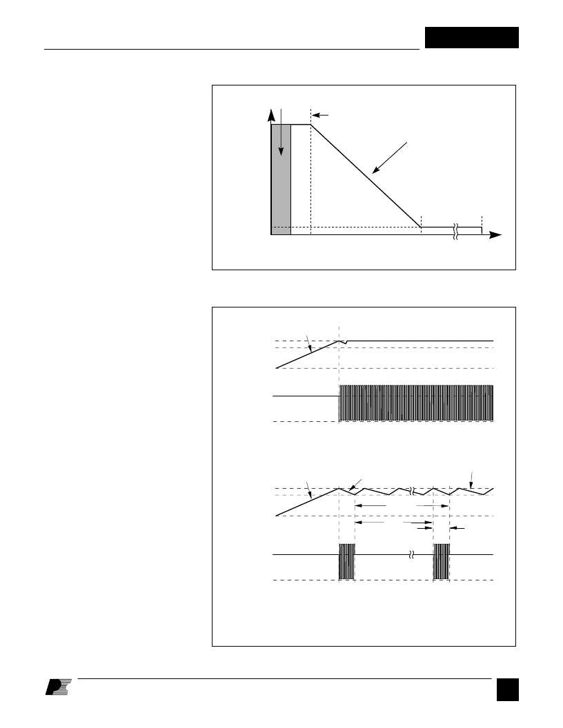
During normal operation, the internal
output MOSFET duty cycle linearly
decreases with increasing CONTROL
pin current as shown in Figure 4. To
implement all the required control, bias,
and protection functions, the DRAIN
and CONTROL pins each perform
several functions as described below.
Refer to Figure 2 for a block diagram
and Figure 6 for timing and voltage
waveforms of the
TOPSwitch
integrated
circuit.
Control Voltage Supply
CONTROL pin voltage V
is the supply
or bias voltage for the controller and
driver circuitry. An external bypass
capacitor closely connected between the
CONTROL and SOURCE pins is
required to supply the gate drive current.
The total amount of capacitance
connected to this pin (C
) also sets the
auto-restart timing as well as control
loop compensation. V
is regulated in
either of two modes of operation.
Hysteretic regulation is used for initial
start-up and overload operation. Shunt
regulation is used to separate the duty
cycle error signal from the control circuit
supply current. During start-up, V
C
current is supplied from a high-voltage
switched current source connected
internally between the DRAIN and
CONTROL pins. The current source
provides sufficient current to supply the
control circuitry as well as charge the
total external capacitance (C
T
).
PI-1691-112895
DMAX
DMIN
ICD1
D
IC (mA)
2.5
6.5
45
Slope = PWM Gain
-16%/mA
IB
Auto-restart
Figure 4. Relationship of Duty Cycle to CONTROL Pin Current.
Figure 5. Start-up Waveforms for (a) Normal Operation and (b) Auto-restart.
DRAIN
0
VIN
VC
0
4.7 V
5.7 V
8 Cycles
95%
5%
Off
Switching
Switching
Off
IC
Charging CT
ICD1
Discharging CT
ICD2
Discharging CT
IC
Charging CT
Off
PI-1124A-060694
DRAIN
0
VIN
VC
0
4.7 V
5.7 V
Off
Switching
(b)
(a)
C
T
is the total external capacitance
connected to the CONTROL pin
相關PDF資料 |
PDF描述 |
|---|---|
| TOP102YAI | Analog IC |
| TOP102YAI* | 0-60 W TOPSwitch using a 100/110 VAC input |
| TOP103YAI | Analog IC |
| TOP103YAI* | 0-60 W TOPSwitch using a 100/110 VAC input |
| TOP104YAI* | 0-60 W TOPSwitch using a 100/110 VAC input |
相關代理商/技術參數 |
參數描述 |
|---|---|
| TOP101YN | 功能描述:交流/直流開關轉換器 15-35 W 100/110 VAC RoHS:否 制造商:STMicroelectronics 輸出電壓:800 V 輸入/電源電壓(最大值):23.5 V 輸入/電源電壓(最小值):11.5 V 開關頻率:115 kHz 電源電流:1.6 mA 工作溫度范圍:- 40 C to + 150 C 安裝風格:SMD/SMT 封裝 / 箱體:SSO-10 封裝:Reel |
| TOP102YAI | 功能描述:交流/直流開關轉換器 20-45 W 100/110 VAC RoHS:否 制造商:STMicroelectronics 輸出電壓:800 V 輸入/電源電壓(最大值):23.5 V 輸入/電源電壓(最小值):11.5 V 開關頻率:115 kHz 電源電流:1.6 mA 工作溫度范圍:- 40 C to + 150 C 安裝風格:SMD/SMT 封裝 / 箱體:SSO-10 封裝:Reel |
| TOP102YI | 制造商:POWERINT 制造商全稱:Power Integrations, Inc. 功能描述:Three-terminal Off-line PWM Switch |
發(fā)布緊急采購,3分鐘左右您將得到回復。