- 您現(xiàn)在的位置:買賣IC網(wǎng) > PDF目錄20492 > TOOLSTICK717MPP (Silicon Laboratories Inc)PLATFORM PROG TOOLSTCK F717 PDF資料下載
參數(shù)資料
| 型號(hào): | TOOLSTICK717MPP |
| 廠商: | Silicon Laboratories Inc |
| 文件頁數(shù): | 12/306頁 |
| 文件大?。?/td> | 0K |
| 描述: | PLATFORM PROG TOOLSTCK F717 |
| 標(biāo)準(zhǔn)包裝: | 1 |
| 系列: | ToolStick |
| 類型: | 微控制器編程器 |
| 適用于相關(guān)產(chǎn)品: | C8051F717 |
| 所含物品: | 板 |
| 產(chǎn)品目錄頁面: | 626 (CN2011-ZH PDF) |
| 其它名稱: | 336-1967 |
第1頁第2頁第3頁第4頁第5頁第6頁第7頁第8頁第9頁第10頁第11頁當(dāng)前第12頁第13頁第14頁第15頁第16頁第17頁第18頁第19頁第20頁第21頁第22頁第23頁第24頁第25頁第26頁第27頁第28頁第29頁第30頁第31頁第32頁第33頁第34頁第35頁第36頁第37頁第38頁第39頁第40頁第41頁第42頁第43頁第44頁第45頁第46頁第47頁第48頁第49頁第50頁第51頁第52頁第53頁第54頁第55頁第56頁第57頁第58頁第59頁第60頁第61頁第62頁第63頁第64頁第65頁第66頁第67頁第68頁第69頁第70頁第71頁第72頁第73頁第74頁第75頁第76頁第77頁第78頁第79頁第80頁第81頁第82頁第83頁第84頁第85頁第86頁第87頁第88頁第89頁第90頁第91頁第92頁第93頁第94頁第95頁第96頁第97頁第98頁第99頁第100頁第101頁第102頁第103頁第104頁第105頁第106頁第107頁第108頁第109頁第110頁第111頁第112頁第113頁第114頁第115頁第116頁第117頁第118頁第119頁第120頁第121頁第122頁第123頁第124頁第125頁第126頁第127頁第128頁第129頁第130頁第131頁第132頁第133頁第134頁第135頁第136頁第137頁第138頁第139頁第140頁第141頁第142頁第143頁第144頁第145頁第146頁第147頁第148頁第149頁第150頁第151頁第152頁第153頁第154頁第155頁第156頁第157頁第158頁第159頁第160頁第161頁第162頁第163頁第164頁第165頁第166頁第167頁第168頁第169頁第170頁第171頁第172頁第173頁第174頁第175頁第176頁第177頁第178頁第179頁第180頁第181頁第182頁第183頁第184頁第185頁第186頁第187頁第188頁第189頁第190頁第191頁第192頁第193頁第194頁第195頁第196頁第197頁第198頁第199頁第200頁第201頁第202頁第203頁第204頁第205頁第206頁第207頁第208頁第209頁第210頁第211頁第212頁第213頁第214頁第215頁第216頁第217頁第218頁第219頁第220頁第221頁第222頁第223頁第224頁第225頁第226頁第227頁第228頁第229頁第230頁第231頁第232頁第233頁第234頁第235頁第236頁第237頁第238頁第239頁第240頁第241頁第242頁第243頁第244頁第245頁第246頁第247頁第248頁第249頁第250頁第251頁第252頁第253頁第254頁第255頁第256頁第257頁第258頁第259頁第260頁第261頁第262頁第263頁第264頁第265頁第266頁第267頁第268頁第269頁第270頁第271頁第272頁第273頁第274頁第275頁第276頁第277頁第278頁第279頁第280頁第281頁第282頁第283頁第284頁第285頁第286頁第287頁第288頁第289頁第290頁第291頁第292頁第293頁第294頁第295頁第296頁第297頁第298頁第299頁第300頁第301頁第302頁第303頁第304頁第305頁第306頁
Rev. 1.0
109
C8051F70x/71x
17.1. Program Memory
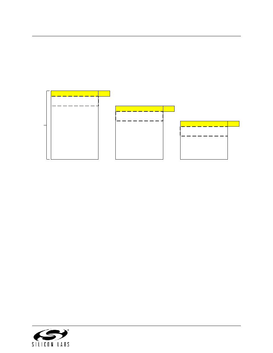
The members of the C8051F70x/71x device family contain 16 kB (C8051F702/3/6/7 and C8051F16/7),
15 kB (C8051F700/1/4/5), or 8 kB (C8051F708/9 and C8051F710/1/2/3/4/5) of re-programmable Flash
memory that can be used as non-volatile program or data storage. The last byte of user code space is
used as the security lock byte (0x3FFF on 16 kB devices, 0x3BFF on 15 kB devices and 0x1FFF on 8 kB
devices).
Figure 17.2. Flash Program Memory Map
17.1.1. MOVX Instruction and Program Memory
The MOVX instruction in an 8051 device is typically used to access external data memory. On the
C8051F70x/71x devices, the MOVX instruction is normally used to read and write on-chip XRAM, but can
be re-configured to write and erase on-chip Flash memory space. MOVC instructions are always used to
read Flash memory, while MOVX write instructions are used to erase and write Flash. This Flash access
feature provides a mechanism for the C8051F70x/71x to update program code and use the program mem-
ory space for non-volatile data storage. Refer to Section “22. Flash Memory” on page 148 for further
details.
17.2. EEPROM Memory
The C8051F700/1/4/5/8/9 and C8051F712/3 contain EEPROM emulation hardware, which uses Flash
memory to emulate a 32-byte EEPROM memory space for non-volatile data storage. The EEPROM data is
accessed through a RAM buffer for increased speed. More details about the EEPROM can be found in
17.3. Data Memory
The C8051F70x/71x device family includes 512 bytes of RAM data memory. 256 bytes of this memory is
mapped into the internal RAM space of the 8051. 256 bytes of this memory is on-chip “external” memory.
The data memory map is shown in Figure 17.1 for reference.
17.3.1. Internal RAM
There are 256 bytes of internal RAM mapped into the data memory space from 0x00 through 0xFF. The
lower 128 bytes of data memory are used for general purpose registers and scratch pad memory. Either
direct or indirect addressing may be used to access the lower 128 bytes of data memory. Locations 0x00
through 0x1F are addressable as four banks of general purpose registers, each bank consisting of eight
Lock Byte
0x0000
0x3FFF
0x3FFE
FLASH
memory
or
g
a
ni
z
ed
in
512
-by
te
p
age
s
0x3E00
Flash Memory Space
Lock Byte Page
Lock Byte
0x0000
0x3BFF
0x3BFE
0x3A00
Flash Memory Space
Lock Byte Page
Lock Byte
0x0000
0x1FFF
0x1FFE
0x1E00
Flash Memory Space
Lock Byte Page
C8051F702/3/6/7 and
C8051F716/7
C8051F700/1/4/5
C8051F708/9 and
C8051F710/1/2/3/4/5
相關(guān)PDF資料 |
PDF描述 |
|---|---|
| ECC24DJBN | CONN EDGECARD 48PS .100 PRESSFIT |
| VI-J3P-CW-F4 | CONVERTER MOD DC/DC 13.8V 100W |
| RBC06DRAS | CONN EDGECARD 12POS R/A .100 SLD |
| VE-2NX-CX-S | CONVERTER MOD DC/DC 5.2V 75W |
| RCC08DRAN | CONN EDGECARD 16POS R/A .100 SLD |
相關(guān)代理商/技術(shù)參數(shù) |
參數(shù)描述 |
|---|---|
| TOOLSTICK800DC | 功能描述:子卡和OEM板 ToolStick C8051F800 Daughter Card RoHS:否 制造商:BeagleBoard by CircuitCo 產(chǎn)品:BeagleBone LCD4 Boards 用于:BeagleBone - BB-Bone - Open Source Development Kit |
| TOOLSTICK800MPP | 功能描述:插座和適配器 Toolstick F8xx -GM MCUs RoHS:否 制造商:Silicon Labs 產(chǎn)品:Adapter 用于:EM35x |
| TOOLSTICK800QPP | 功能描述:插座和適配器 Toolstick F8xx -GU MCUs RoHS:否 制造商:Silicon Labs 產(chǎn)品:Adapter 用于:EM35x |
| TOOLSTICK800SPP | 功能描述:插座和適配器 Toolstick F8xx -GS MCUs RoHS:否 制造商:Silicon Labs 產(chǎn)品:Adapter 用于:EM35x |
| TOOLSTICK850-B-DC | 制造商:Silicon Laboratories Inc 功能描述:DAUGHTERCARD TOOLSTICK C8051F850 |
發(fā)布緊急采購,3分鐘左右您將得到回復(fù)。