- 您現(xiàn)在的位置:買(mǎi)賣(mài)IC網(wǎng) > PDF目錄382658 > TNY268PG 4-23 W TinySwitch-II family of energy efficient. PDF資料下載
參數(shù)資料
| 型號(hào): | TNY268PG |
| 英文描述: | 4-23 W TinySwitch-II family of energy efficient. |
| 中文描述: | 4-23糯的TinySwitch -Ⅱ系列高效的能源。 |
| 文件頁(yè)數(shù): | 3/24頁(yè) |
| 文件大?。?/td> | 200K |
| 代理商: | TNY268PG |
第1頁(yè)第2頁(yè)當(dāng)前第3頁(yè)第4頁(yè)第5頁(yè)第6頁(yè)第7頁(yè)第8頁(yè)第9頁(yè)第10頁(yè)第11頁(yè)第12頁(yè)第13頁(yè)第14頁(yè)第15頁(yè)第16頁(yè)第17頁(yè)第18頁(yè)第19頁(yè)第20頁(yè)第21頁(yè)第22頁(yè)第23頁(yè)第24頁(yè)

3
TNY264/266-268
C
4/03
TinySwitch-II
Functional Description
TinySwitch-II
combines a high voltage power MOSFET switch
with a power supply controller in one device. Unlike conventional
PWM (Pulse Width Modulator) controllers,
TinySwitch-II
uses
a simple ON/OFF control to regulate the output voltage.
The
TinySwitch-II
controller consists of an Oscillator, Enable
Circuit (Sense and Logic), Current Limit State Machine, 5.8 V
Regulator, Bypass pin Under-Voltage Circuit, Over
Temperature Protection, Current Limit Circuit, Leading Edge
Blanking and a 700 V power MOSFET.
TinySwitch-II
incorporates additional circuitry for Line Under-Voltage Sense,
Auto-Restart and Frequency Jitter. Figure 2 shows the functional
block diagram with the most important features.
Oscillator
The typical oscillator frequency is internally set to an average
of 132 kHz. Two signals are generated from the oscillator: the
Maximum Duty Cycle signal (DC
) and the Clock signal that
indicates the beginning of each cycle.
The
TinySwitch-II
oscillator incorporates circuitry that
introduces a small amount of frequency jitter, typically 8 kHz
peak-to-peak, to minimize EMI emission. The modulation rate
of the frequency jitter is set to 1 kHz to optimize EMI reduction
for both average and quasi-peak emissions. The frequency jitter
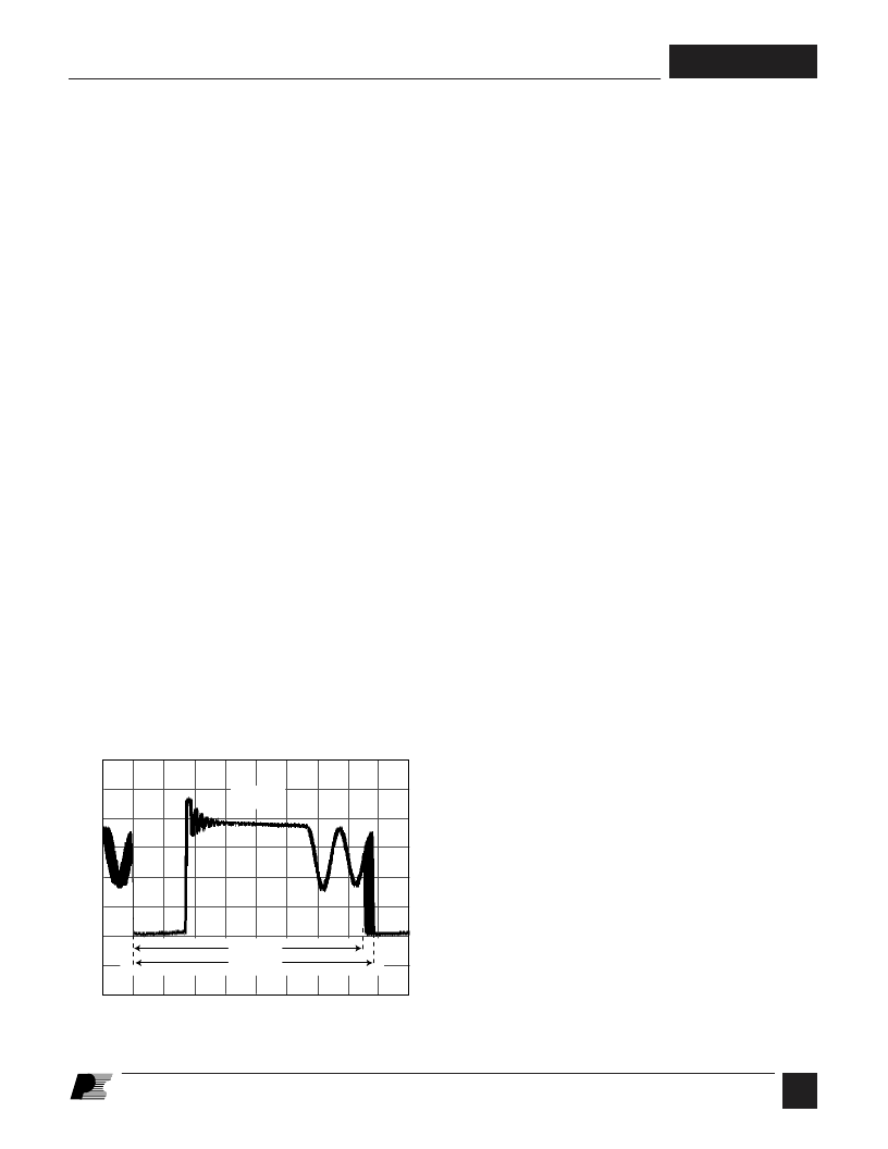
should be measured with the oscilloscope triggered at the
falling edge of the DRAIN waveform. The waveform in Figure 4
illustrates the frequency jitter of the
TinySwitch-II
.
Enable Input and Current Limit State Machine
The enable input circuit at the EN/UV pin consists of a low
impedance source follower output set at 1.0 V. The current
through the source follower is limited to 240
μ
A. When the
current out of this pin exceeds 240
μ
A, a low logic level
(disable) is generated at the output of the enable circuit. This
enable circuit output is sampled at the beginning of each cycle
on the rising edge of the clock signal. If high, the power
MOSFET is turned on for that cycle (enabled). If low, the power
MOSFET remains off (disabled). Since the sampling is done
only at the beginning of each cycle, subsequent changes in the
EN/UV pin voltage or current during the remainder of the cycle
are ignored.
The Current Limit State Machine reduces the current limit by
discrete amounts at light loads when
TinySwitch-II
is likely to
switch in the audible frequency range. The lower current limit
raises the effective switching frequency above the audio range
and reduces the transformer flux density including the associated
audible noise. The state machine monitors the sequence of
EN/UV pin voltage levels to determine the load condition and
adjusts the current limit level accordingly in discrete amounts.
Under most operating conditions (except when close to no-
load), the low impedance of the source follower keeps the
voltage on the EN/UV pin from going much below 1.0 V in the
disabled state. This improves the response time of the optocoupler
that is usually connected to this pin.
5.8 V Regulator and 6.3 V Shunt Voltage Clamp
The 5.8 V regulator charges the bypass capacitor connected to
the BYPASS pin to 5.8 V by drawing a current from the voltage
on the DRAIN pin, whenever the MOSFET is off. The
BYPASS pin is the internal supply voltage node for the
TinySwitch-II
. When the MOSFET is on, the
TinySwitch-II
operates from the energy stored in the bypass capacitor.
Extremely low power consumption of the internal circuitry
allows
TinySwitch-II
to operate continuously from current it
takes from the DRAIN pin. A bypass capacitor value of 0.1
μ
F
is sufficient for both high frequency decoupling and energy
storage.
In addition, there is a 6.3 V shunt regulator clamping the
BYPASS pin at 6.3 V when current is provided to the BYPASS
pin through an external resistor. This facilitates powering of
TinySwitch-II
externally through a bias winding to decrease the
no load consumption to about 50 mW.
BYPASS Pin Under-Voltage
The BYPASS pin under-voltage circuitry disables the power
MOSFET when the BYPASS pin voltage drops below 4.8 V.
Once the BYPASS pin voltage drops below 4.8 V, it must rise
back to 5.8 V to enable (turn-on) the power MOSFET.
Figure 4. Frequency Jitter.
P
0
5
10
Time (
μ
s)
0
100
200
400
500
600
300
VDRAIN
136 kHz
128 kHz
相關(guān)PDF資料 |
PDF描述 |
|---|---|
| TO0812LN | Analog IC |
| TO1217LN | Analog IC |
| TO1724LN | Analog IC |
| TO124P | NADELFEILENSATZ 6TLG 140MM |
| TO14D-8042-4 | COLOUR TFT LCD KIT |
相關(guān)代理商/技術(shù)參數(shù) |
參數(shù)描述 |
|---|---|
| TNY268PN | 功能描述:交流/直流開(kāi)關(guān)轉(zhuǎn)換器 15W 85-265 VAC 19W/230 VAC RoHS:否 制造商:STMicroelectronics 輸出電壓:800 V 輸入/電源電壓(最大值):23.5 V 輸入/電源電壓(最小值):11.5 V 開(kāi)關(guān)頻率:115 kHz 電源電流:1.6 mA 工作溫度范圍:- 40 C to + 150 C 安裝風(fēng)格:SMD/SMT 封裝 / 箱體:SSO-10 封裝:Reel |
| TNY268PN-TL | 制造商:POWERINT 制造商全稱(chēng):Power Integrations, Inc. 功能描述:Enhanced, Energy Efficient, Low Power Off-line Switcher |
| TNY268PTL | 制造商:POWERINT 制造商全稱(chēng):Power Integrations, Inc. 功能描述:Enhanced, Energy Efficient, Low Power Off-line Switcher |
| TNY274 | 制造商:POWERINT 制造商全稱(chēng):Power Integrations, Inc. 功能描述:Energy Efficient, Off-Line Switcher with Enhanced Flexibility and Extended Power Range |
| TNY274_09 | 制造商:POWERINT 制造商全稱(chēng):Power Integrations, Inc. 功能描述:Energy-Effi cient, Off-Line Switcher With Enhanced Flexibility and Extended Power Range |
發(fā)布緊急采購(gòu),3分鐘左右您將得到回復(fù)。