- 您現(xiàn)在的位置:買賣IC網(wǎng) > PDF目錄384019 > TMS320F28044ZGMQ (Texas Instruments, Inc.) Digital Signal Processor PDF資料下載
參數(shù)資料
| 型號: | TMS320F28044ZGMQ |
| 廠商: | Texas Instruments, Inc. |
| 元件分類: | 數(shù)字信號處理 |
| 英文描述: | Digital Signal Processor |
| 中文描述: | 數(shù)字信號處理器 |
| 文件頁數(shù): | 36/107頁 |
| 文件大小: | 784K |
| 代理商: | TMS320F28044ZGMQ |
第1頁第2頁第3頁第4頁第5頁第6頁第7頁第8頁第9頁第10頁第11頁第12頁第13頁第14頁第15頁第16頁第17頁第18頁第19頁第20頁第21頁第22頁第23頁第24頁第25頁第26頁第27頁第28頁第29頁第30頁第31頁第32頁第33頁第34頁第35頁當前第36頁第37頁第38頁第39頁第40頁第41頁第42頁第43頁第44頁第45頁第46頁第47頁第48頁第49頁第50頁第51頁第52頁第53頁第54頁第55頁第56頁第57頁第58頁第59頁第60頁第61頁第62頁第63頁第64頁第65頁第66頁第67頁第68頁第69頁第70頁第71頁第72頁第73頁第74頁第75頁第76頁第77頁第78頁第79頁第80頁第81頁第82頁第83頁第84頁第85頁第86頁第87頁第88頁第89頁第90頁第91頁第92頁第93頁第94頁第95頁第96頁第97頁第98頁第99頁第100頁第101頁第102頁第103頁第104頁第105頁第106頁第107頁
www.ti.com
3.6.1
OSC and PLL Block
X1
XCLKIN
(3.3-V clock input)
On chip
oscillator
X2
xor
PLLSTS[OSCOFF]
OSCCLK
PLL
VCOCLK
4-bit PLL Select (PLLCR)
OSCCLK or
VCOCLK
CLKIN
OSCCLK
0
PLLSTS[PLLOFF]
n
n
≠
0
/2
PLLSTS[CLKINDIV]
External Clock Signal
(Toggling 0V
DDIO
)
XCLKIN
X2
NC
X1
External Clock Signal
(Toggling 0V
DD
)
XCLKIN
X2
NC
X1
C
L1
X2
X1
Crystal
C
L2
XCLKIN
TMS320F28044
Digital Signal Processor
SPRS357B–AUGUST 2006–REVISED MAY 2007
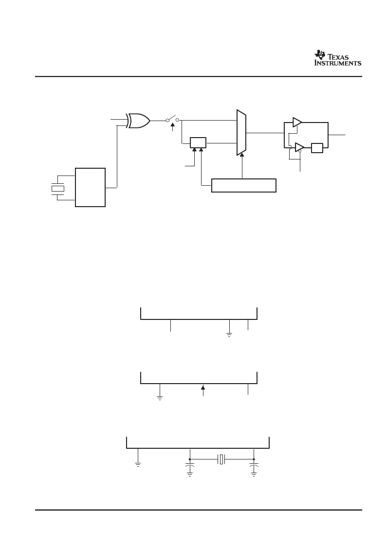
Figure 3-6
shows the OSC and PLL block on the F28044.
Figure 3-6. OSC and PLL Block Diagram
The on-chip oscillator circuit enables a crystal/resonator to be attached to the F28044 device using the X1
and X2 pins. If the on-chip oscillator is not used, an external oscillator can be used in either one of the
following configurations:
1. A 3.3-V external oscillator can be directly connected to the XCLKIN pin. The X2 pin should be left
unconnected and the X1 pin tied low. The logic-high level in this case should not exceed V
DDIO
.
2. A 1.8-V external oscillator can be directly connected to the X1 pin. The X2 pin should be left
unconnected and the XCLKIN pin tied low. The logic-high level in this case should not exceed V
DD
.
The three possible input-clock configurations are shown in
Figure 3-7
through
Figure 3-9
Figure 3-7. Using a 3.3-V External Oscillator
Figure 3-8. Using a 1.8-V External Oscillator
Figure 3-9. Using the Internal Oscillator
36
Functional Overview
Submit Documentation Feedback
相關PDF資料 |
PDF描述 |
|---|---|
| TMS320F28044ZGMS | Digital Signal Processor |
| TMX320F28044GGMQ | Digital Signal Processor |
| TMX320F28044GGMS | Digital Signal Processor |
| TMX320F28044PZQ | Digital Signal Processor |
| TMX320F28044PZS | Digital Signal Processor |
相關代理商/技術(shù)參數(shù) |
參數(shù)描述 |
|---|---|
| TMS320F28045PZA | 制造商:Texas Instruments 功能描述:- Trays |
| TMS320F28045PZS | 制造商:Texas Instruments 功能描述:- Trays |
| TMS320F28050PNQ | 制造商:Texas Instruments 功能描述:GIZMO |
| TMS320F28050PNS | 制造商:Texas Instruments 功能描述:GIZMO |
| TMS320F28050PNT | 制造商:Texas Instruments 功能描述:GIZMO |
發(fā)布緊急采購,3分鐘左右您將得到回復。