- 您現(xiàn)在的位置:買賣IC網(wǎng) > PDF目錄384014 > TMC2250AG1C (FAIRCHILD SEMICONDUCTOR CORP) Matrix Multiplier 12 x 10 bit, 50 MHz PDF資料下載
參數(shù)資料
| 型號(hào): | TMC2250AG1C |
| 廠商: | FAIRCHILD SEMICONDUCTOR CORP |
| 元件分類: | 數(shù)字信號(hào)處理外設(shè) |
| 英文描述: | Matrix Multiplier 12 x 10 bit, 50 MHz |
| 中文描述: | 12-BIT, DSP-MULTIPLIER, CPGA120 |
| 封裝: | CERAMIC, PGA-120 |
| 文件頁(yè)數(shù): | 7/23頁(yè) |
| 文件大小: | 186K |
| 代理商: | TMC2250AG1C |
第1頁(yè)第2頁(yè)第3頁(yè)第4頁(yè)第5頁(yè)第6頁(yè)當(dāng)前第7頁(yè)第8頁(yè)第9頁(yè)第10頁(yè)第11頁(yè)第12頁(yè)第13頁(yè)第14頁(yè)第15頁(yè)第16頁(yè)第17頁(yè)第18頁(yè)第19頁(yè)第20頁(yè)第21頁(yè)第22頁(yè)第23頁(yè)
TMC2250A
PRODUCT SPECIFICATION
REV. 1.0.2 10/25/00
7
Notes:
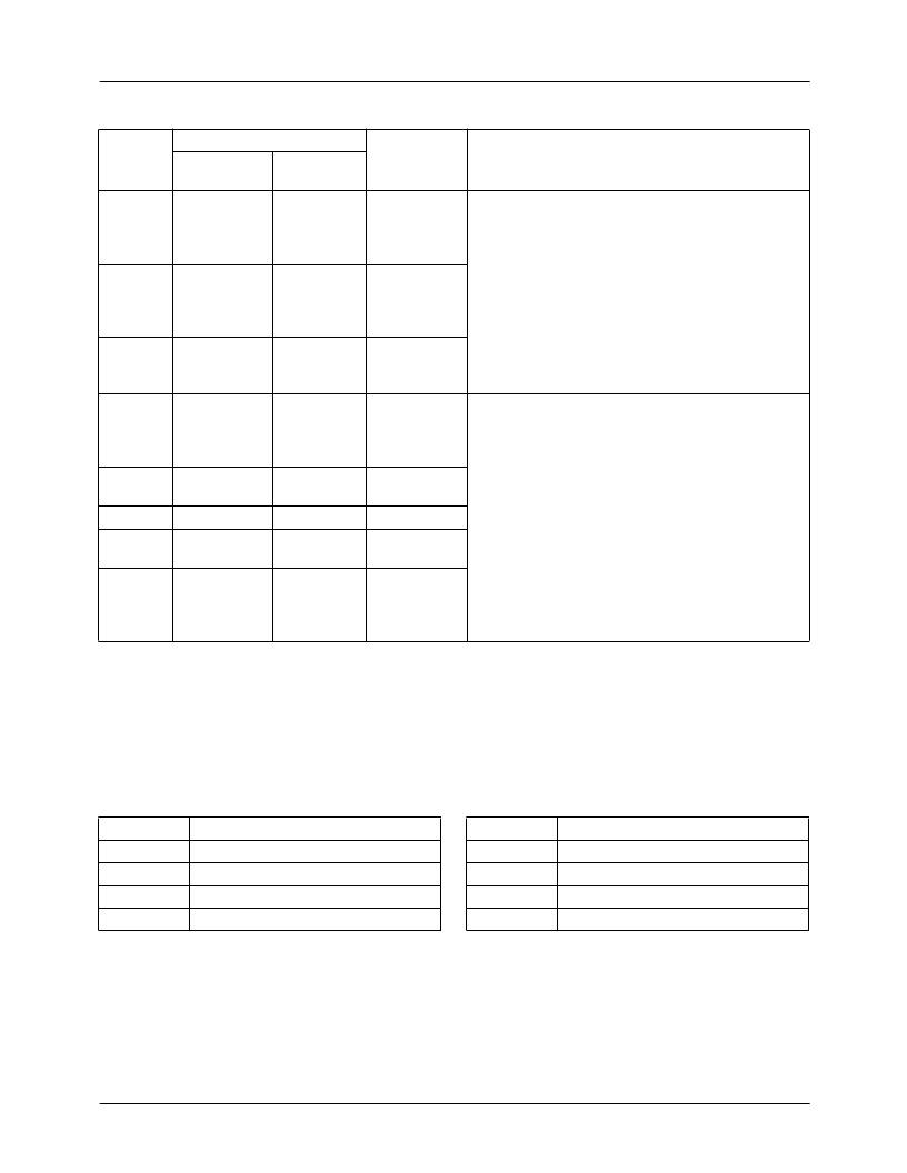
1. The output ports X, Y, Z and CASOUT, and input port CASIN are internally reconfigured by the device as required for each
mode of the device. The multiple-function pins have names which are combinations of these titles, as appropriate.
2. The output drivers on pins XC
11-0
and YC
11-8
are not necessarily disabled until after the first rising edge of CLK following
power-up. If these pins are to be tied to other output drivers, to each other, or to ground or V
DD
, the user should ensure that
a clock pulse arrives within a few seconds of power-up, to avoid bus contention.
KA
9-0
K13, J11, K12,
L13, L12, K11,
M13, M12,
L11, N13
M11, L10,
N12, N11,
M10, L9, N10,
M9, N9, L8
M8, N8, N7,
M7, N6, M6,
N5, M5, N4, L5
B4, A3, A2, B3,
A1, C3, B2, B1,
D3, C2, C1, D2
69, 68, 67, 66,
65, 64, 63, 62,
61, 60
Coefficient
Input A1, A2,
A3
Data presented to the 10-bit registered coefficient
input ports KA, KB and KC are latched three at a time
into the internal coefficient storage register set
indicated by the Coefficient Write Enable CWE
1,0
on
the next clock, as shown in Table 4.
KB
9-0
59, 58, 57, 56,
55, 54, 53, 52,
51, 50
Coefficient
Input B1, B2,
B3
KC
9-0
49, 48, 47, 45,
44, 43, 41, 40,
39, 38
115, 116,
117, 119,
120, 1, 2, 3, 4,
5, 6, 7
Coefficient
Input B1, B2,
B3
CASIN
15-4
/
Output X
XC
11-0
In all modes except Mode 00, the x port and four bits
of the Y output port are reconfigured as the 16-bit
registered Cascade Input port CASIN
15-0
. Data
presented to this input will be added to the weighted
sums of the data words which were presented to the
input ports (A, B and C).
In the matrix multiply mode, data are available at the
12-bit registered output ports X, Y AND Z t
DO
after
every clock. These ports are reconfigured in the
filtering modes as 16-bit Cascade Input and Output
ports.CASOUT
15-0
In all modes except Mode 00, the Z port and four bits
of the Y output port are reconfigured as the 16-bit
registered Cascade Output port CASOUT
15-0
.
YC
11-8
D1, E2, E1, F2 9, 10, 11, 13
CASIN
3-0
/
Output Y
11-0
Y
7-4
YC
3-0
F1, G2, G1, H1 14, 15, 17, 18 Output
7-4
only
K1, J2, J1, H2 23, 22, 21, 19 CASOUT
3-0
/
Output Y
3-0
CASOUT
15-4
/
Output Z
11-0
ZC
11-0
M4, N3, M3,
N2, M2, L3,
N1, L2, K3,
M1, L1, K2
37, 36, 35, 33,
32, 31, 30, 29,
28, 27, 26, 25
Pin Descriptions
(continued)
Pin Name
Pin Number
Function
Pin Description
CPGA/PPGA/
MPGA
MQFP
Table 3. Con
fi
guration Mode Word
Table 4. Coef
fi
cient Write Enable Word
MODE
1,0
00
01
10
11
Con
fi
guration Mode
3 x 3 Matrix Multiply
9-Tap One Dimensional FIR
3 x 3 -Pixel Convolver
4 x 2 -Pixel Convolver
CWE
1,0
00
01
10
11
Coef
fi
cient Set Selected
Hold all registers
Update KA1, KB1, KC1
Update KA2, KB2, KC2
Update KA3, KB3, KC3
相關(guān)PDF資料 |
PDF描述 |
|---|---|
| TMC2250AG1C2 | Matrix Multiplier 12 x 10 bit, 50 MHz |
| TMC2250AG1C3 | Matrix Multiplier 12 x 10 bit, 50 MHz |
| TMC2250AH6C | JT 7C 7#20 PIN PLUG |
| TMC2250AH6C2 | Matrix Multiplier 12 x 10 bit, 50 MHz |
| TMC2250AH6C3 | Circular Connector; No. of Contacts:13; Series:MS27473; Body Material:Aluminum; Connecting Termination:Crimp; Connector Shell Size:10; Circular Contact Gender:Socket; Circular Shell Style:Straight Plug; Insert Arrangement:10-35 RoHS Compliant: No |
相關(guān)代理商/技術(shù)參數(shù) |
參數(shù)描述 |
|---|---|
| TMC2250AG1C2 | 制造商:CADEKA 制造商全稱:CADEKA 功能描述:Matrix Multiplier 12 x 10 bit, 50 MHz |
| TMC2250AG1C3 | 制造商:CADEKA 制造商全稱:CADEKA 功能描述:Matrix Multiplier 12 x 10 bit, 50 MHz |
| TMC2250AH5C | 制造商:Rochester Electronics LLC 功能描述:- Bulk |
| TMC2250AH5C2 | 制造商:FAIRCHILD 制造商全稱:Fairchild Semiconductor 功能描述:Matrix Multiplier 12 x 10 bit, 50 MHz |
| TMC2250AH5C3 | 制造商:CADEKA 制造商全稱:CADEKA 功能描述:Matrix Multiplier 12 x 10 bit, 50 MHz |
發(fā)布緊急采購(gòu),3分鐘左右您將得到回復(fù)。