- 您現(xiàn)在的位置:買賣IC網(wǎng) > PDF目錄384012 > TMC22091KHC (FAIRCHILD SEMICONDUCTOR CORP) Digital Video Encoders/Layering Engine PDF資料下載
參數(shù)資料
| 型號(hào): | TMC22091KHC |
| 廠商: | FAIRCHILD SEMICONDUCTOR CORP |
| 元件分類: | 顏色信號(hào)轉(zhuǎn)換 |
| 英文描述: | Digital Video Encoders/Layering Engine |
| 中文描述: | COLOR SIGNAL ENCODER, PQFP100 |
| 封裝: | 3.20 MM HEIGHT, MQFP-100 |
| 文件頁(yè)數(shù): | 53/60頁(yè) |
| 文件大小: | 293K |
| 代理商: | TMC22091KHC |
第1頁(yè)第2頁(yè)第3頁(yè)第4頁(yè)第5頁(yè)第6頁(yè)第7頁(yè)第8頁(yè)第9頁(yè)第10頁(yè)第11頁(yè)第12頁(yè)第13頁(yè)第14頁(yè)第15頁(yè)第16頁(yè)第17頁(yè)第18頁(yè)第19頁(yè)第20頁(yè)第21頁(yè)第22頁(yè)第23頁(yè)第24頁(yè)第25頁(yè)第26頁(yè)第27頁(yè)第28頁(yè)第29頁(yè)第30頁(yè)第31頁(yè)第32頁(yè)第33頁(yè)第34頁(yè)第35頁(yè)第36頁(yè)第37頁(yè)第38頁(yè)第39頁(yè)第40頁(yè)第41頁(yè)第42頁(yè)第43頁(yè)第44頁(yè)第45頁(yè)第46頁(yè)第47頁(yè)第48頁(yè)第49頁(yè)第50頁(yè)第51頁(yè)第52頁(yè)當(dāng)前第53頁(yè)第54頁(yè)第55頁(yè)第56頁(yè)第57頁(yè)第58頁(yè)第59頁(yè)第60頁(yè)
PRODUCT SPECIFICATION
TMC22091/TMC22191
53
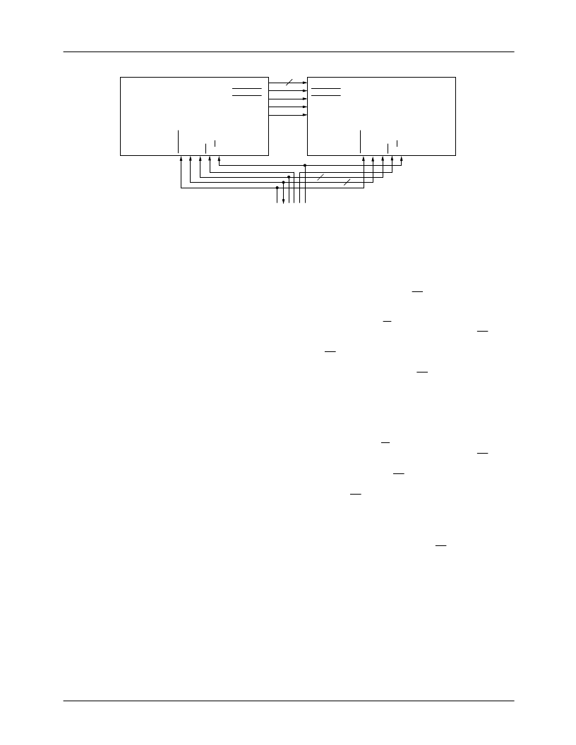
Figure 37. TMC22x91-to-TMC22071 Interface Circuit
2
8
8
27009A
CVBS7-0
GHSYNC
GVSYNC
PXCK
R
D
A
C
R
LDV
CVBS7-0
GHSYNC
GVSYNC
PXCK
LDV
MICROPROCESSOR
INTERFACE
GENLOCKING VIDEO DIGITIZER
TMC22071
DIGITAL VIDEO ENCODER
TMC22x91
R
D
A
C
R
Printed Circuit Board Layout
Designing with high-performance mixed-signal circuits
demands printed circuits with ground planes. Overall system
performance is strongly influenced by the board layout.
Capacitive coupling from digital to analog circuits may
result in poor picture quality. Consider the following sugges-
tions when doing the layout:
Keep analog traces (COMP, V
REF
, R
REF
) as short and as
far from all digital signals as possible.
The power plane for the TMC22x91 should be separate
from that which supplies other digital circuitry. A single
power plane should be used for all of the V
DD
pins. If the
power supply for the TMC22x91 is the same for the
system’s digital circuitry, power to the TMC22x91 should
be filtered with ferrite beads and 0.1
μ
F capacitors to
reduce noise.
The ground plane should be solid, not cross-hatched.
Connections to the ground plane should be very short.
Decoupling capacitors should be applied liberally to V
DD
pins. For best results, use 0.1
μ
F capacitor in
parallel with 47
μ
F capacitors. Lead lengths should be
minimized. Ceramic chip capacitors are the best choice.
The PXCK should be handled carefully. Jitter and noise
on this clock or its ground reference will translate to noise
on the video outputs. Terminate the clock line carefully to
eliminate overshoot and ringing.
Microprocessor I/O Operations
Various CLUT Read/Write operations are shown in Table 17.
Each step in the table requires a CS pulse (falling edge fol-
lowed by a rising edge) to execute.
For Write operations, R/W and A
1-0
must conform to setup
and hold timing with respect to the falling edge of CS. D
7-0
must meet setup and hold timing with respect to the rising
edge of CS. These timing relationships are illustrated in Fig-
ure 10. When writing data into an internal register (i.e.
CLUT Address Register) an extra CS falling edge is required
to transfer the input data to that register. This requirement is
usually accomplished by executing the next step in the
sequence. If there is no planned next step in the sequence,
executing a Control Register Read step will meet the require-
ment and terminate the sequence.
For Read operations, R/W and A
1-0
must conform to setup
and hold timing with respect to the falling edge of CS. Read
data on D
7-0
is initiated by the falling edge of CS\ and termi-
nated by the rising edge of CS as shown in Figure 11. When
reading Control Registers, valid data appears t
DOM
after the
falling edge of CS. When reading CLUT locations, an extra
CLUT Read step is needed to set up the CLUT Read
sequence. This is accomplished in the table by executing an
extra CLUT Read step just before the CLUT Read sequence
which returns successive d, e, and f data. CLUT Read
sequences must be terminated an extra CS falling edge. This
requirement is usually accomplished by executing the next
I/O step. If there is no planned next step in the sequence,
executing a Control Register Read step will meet the require-
ment and terminate the sequence.
相關(guān)PDF資料 |
PDF描述 |
|---|---|
| TMC22191KHC | Digital Video Encoders/Layering Engine |
| TMC22091R0C | Digital Video Encoders/Layering Engine |
| TMC22191R0C | Digital Video Encoders/Layering Engine |
| TMC22091 | Digital Video Encoders(數(shù)字視頻編碼器) |
| TMC22191 | Digital Video Encoders(數(shù)字視頻編碼器) |
相關(guān)代理商/技術(shù)參數(shù) |
參數(shù)描述 |
|---|---|
| TMC22091R0C | 功能描述:視頻 IC D/V Encoder Layering Engine RoHS:否 制造商:Fairchild Semiconductor 工作電源電壓:5 V 電源電流:80 mA 最大工作溫度:+ 85 C 封裝 / 箱體:TSSOP-28 封裝:Reel |
| TMC22091R0CT | 功能描述:視頻 IC D/V Encoder Layering Engine RoHS:否 制造商:Fairchild Semiconductor 工作電源電壓:5 V 電源電流:80 mA 最大工作溫度:+ 85 C 封裝 / 箱體:TSSOP-28 封裝:Reel |
| TMC22091ROC-T | 制造商:Fairchild Semiconductor Corporation 功能描述: |
| TMC22151AKHC | 制造商:CADEKA 制造商全稱:CADEKA 功能描述:Multistandard Digital Video Decoder Three-Line Adaptive Comb Decoder Family, 8 & 10 bit |
| TMC22151KHC | 制造商:Rochester Electronics LLC 功能描述:- Bulk |
發(fā)布緊急采購(gòu),3分鐘左右您將得到回復(fù)。