- 您現(xiàn)在的位置:買賣IC網(wǎng) > PDF目錄98259 > TLV5619CDWR (TEXAS INSTRUMENTS INC) PARALLEL, WORD INPUT LOADING, 1 us SETTLING TIME, 12-BIT DAC, PDSO20 PDF資料下載
參數(shù)資料
| 型號(hào): | TLV5619CDWR |
| 廠商: | TEXAS INSTRUMENTS INC |
| 元件分類: | DAC |
| 英文描述: | PARALLEL, WORD INPUT LOADING, 1 us SETTLING TIME, 12-BIT DAC, PDSO20 |
| 封裝: | GREEN, PLASTIC, SOIC-20 |
| 文件頁數(shù): | 3/23頁 |
| 文件大?。?/td> | 478K |
| 代理商: | TLV5619CDWR |

www.ti.com
LINEARITY, OFFSET, AND GAIN ERROR SUING SINGLE END SUPPLIES
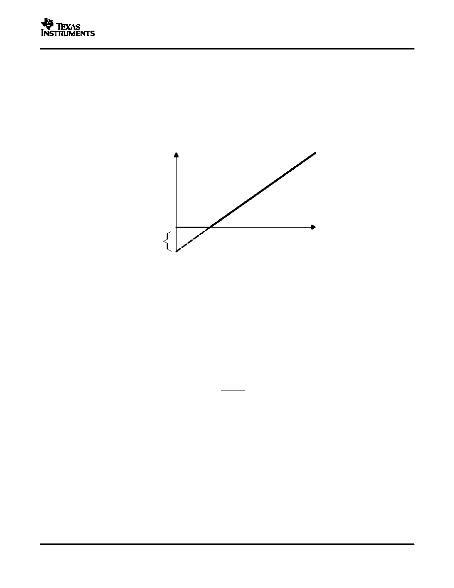
DAC Code
Output
Voltage
0 V
Negative
Offset
GENERAL FUNCTION
2 REF
CODE
0x1000
[V]
TLV5619
SLAS172F – DECEMBER 1997 – REVISED FEBRUARY 2004
APPLICATION INFORMATION (continued)
When an amplifier is operated from a single supply, the voltage offset can still be either positive or negative. With
a positive offset, the output voltage changes on the first code change. With a negative offset the output voltage
may not change with the first code depending on the magnitude of the offset voltage.
The output amplifier attempts to drive the output to a negative voltage. However, because the most negative
supply rail is ground, the output cannot drive below ground and clamps the output at 0 V.
The output voltage remains at zero until the input code value produces a sufficient positive output voltage to
overcome the negative offset voltage, resulting in the transfer function shown in Figure 10.
Figure 10. Effect of Negative Offset (Single Supply)
This offset error, not the linearity error, produces this breakpoint. The transfer function would have followed the
dotted line if the output buffer could drive below the ground rail.
For a DAC, linearity is measured between zero input code (all inputs 0) and full scale code (all inputs 1) after
offset and full scale are adjusted out or accounted for in some way. However, single supply operation does not
allow for adjustment when the offset is negative due to the breakpoint in the transfer function. So the linearity is
measured between full scale code and the lowest code that produces a positive output voltage.
The TLV5619 is a 12-bit, single supply DAC, based on a resistor string architecture. It consists of a parallel
interface, a power down control logic, a resistor string, and a rail-to-rail output buffer. The output voltage (full
scale determined by reference) is given by:
Where REF is the reference voltage and CODE is the digital input value, range 0x000 to 0xFFF. A power on
reset initially puts the internal latches to a defined state (all bits zero).
11
相關(guān)PDF資料 |
PDF描述 |
|---|---|
| TLV5620CN | SERIAL INPUT LOADING, 10 us SETTLING TIME, 8-BIT DAC, PDIP14 |
| TLV5620CD | SERIAL INPUT LOADING, 10 us SETTLING TIME, 8-BIT DAC, PDSO14 |
| TLV5620IN | SERIAL INPUT LOADING, 10 us SETTLING TIME, 8-BIT DAC, PDIP14 |
| TLV5620CDRG4 | SERIAL INPUT LOADING, 10 us SETTLING TIME, 8-BIT DAC, PDSO14 |
| TLV5620CDG4 | SERIAL INPUT LOADING, 10 us SETTLING TIME, 8-BIT DAC, PDSO14 |
相關(guān)代理商/技術(shù)參數(shù) |
參數(shù)描述 |
|---|---|
| TLV5619CDWRG4 | 功能描述:數(shù)模轉(zhuǎn)換器- DAC 12-Bit Sngl Channel DAC RoHS:否 制造商:Texas Instruments 轉(zhuǎn)換器數(shù)量:1 DAC 輸出端數(shù)量:1 轉(zhuǎn)換速率:2 MSPs 分辨率:16 bit 接口類型:QSPI, SPI, Serial (3-Wire, Microwire) 穩(wěn)定時(shí)間:1 us 最大工作溫度:+ 85 C 安裝風(fēng)格:SMD/SMT 封裝 / 箱體:SOIC-14 封裝:Tube |
| TLV5619CPW | 功能描述:數(shù)模轉(zhuǎn)換器- DAC 12-Bit Sngl Channel DAC RoHS:否 制造商:Texas Instruments 轉(zhuǎn)換器數(shù)量:1 DAC 輸出端數(shù)量:1 轉(zhuǎn)換速率:2 MSPs 分辨率:16 bit 接口類型:QSPI, SPI, Serial (3-Wire, Microwire) 穩(wěn)定時(shí)間:1 us 最大工作溫度:+ 85 C 安裝風(fēng)格:SMD/SMT 封裝 / 箱體:SOIC-14 封裝:Tube |
| TLV5619CPW | 制造商:Texas Instruments 功能描述:D/A Converter (D-A) IC |
| TLV5619CPWG4 | 功能描述:數(shù)模轉(zhuǎn)換器- DAC 12-Bit Sngl Channel DAC RoHS:否 制造商:Texas Instruments 轉(zhuǎn)換器數(shù)量:1 DAC 輸出端數(shù)量:1 轉(zhuǎn)換速率:2 MSPs 分辨率:16 bit 接口類型:QSPI, SPI, Serial (3-Wire, Microwire) 穩(wěn)定時(shí)間:1 us 最大工作溫度:+ 85 C 安裝風(fēng)格:SMD/SMT 封裝 / 箱體:SOIC-14 封裝:Tube |
| TLV5619CPWR | 功能描述:數(shù)模轉(zhuǎn)換器- DAC 12-Bit Sngl Channel DAC RoHS:否 制造商:Texas Instruments 轉(zhuǎn)換器數(shù)量:1 DAC 輸出端數(shù)量:1 轉(zhuǎn)換速率:2 MSPs 分辨率:16 bit 接口類型:QSPI, SPI, Serial (3-Wire, Microwire) 穩(wěn)定時(shí)間:1 us 最大工作溫度:+ 85 C 安裝風(fēng)格:SMD/SMT 封裝 / 箱體:SOIC-14 封裝:Tube |
發(fā)布緊急采購,3分鐘左右您將得到回復(fù)。