- 您現(xiàn)在的位置:買賣IC網(wǎng) > PDF目錄383957 > TLV320AIC3106_0706 (Texas Instruments, Inc.) LOW-POWER STEREO AUDIO CODEC FOR PORTABLE AUDIO/TELEPHONY PDF資料下載
參數(shù)資料
| 型號: | TLV320AIC3106_0706 |
| 廠商: | Texas Instruments, Inc. |
| 元件分類: | Codec |
| 英文描述: | LOW-POWER STEREO AUDIO CODEC FOR PORTABLE AUDIO/TELEPHONY |
| 中文描述: | 低功耗立體聲音頻編解碼器的便攜式音頻/電話 |
| 文件頁數(shù): | 22/102頁 |
| 文件大小: | 1259K |
| 代理商: | TLV320AIC3106_0706 |
第1頁第2頁第3頁第4頁第5頁第6頁第7頁第8頁第9頁第10頁第11頁第12頁第13頁第14頁第15頁第16頁第17頁第18頁第19頁第20頁第21頁當前第22頁第23頁第24頁第25頁第26頁第27頁第28頁第29頁第30頁第31頁第32頁第33頁第34頁第35頁第36頁第37頁第38頁第39頁第40頁第41頁第42頁第43頁第44頁第45頁第46頁第47頁第48頁第49頁第50頁第51頁第52頁第53頁第54頁第55頁第56頁第57頁第58頁第59頁第60頁第61頁第62頁第63頁第64頁第65頁第66頁第67頁第68頁第69頁第70頁第71頁第72頁第73頁第74頁第75頁第76頁第77頁第78頁第79頁第80頁第81頁第82頁第83頁第84頁第85頁第86頁第87頁第88頁第89頁第90頁第91頁第92頁第93頁第94頁第95頁第96頁第97頁第98頁第99頁第100頁第101頁第102頁
www.ti.com
I
2
C BUS DEBUG IN A GLITCHED SYSTEM
Occasionally, some systems may encounter noise or glitches on the I
2
C bus. In the unlikely event that this
affects bus performance, then it can be useful to use the I
2
C Debug register. This feature terminates the I
2
C bus
error allowing this I
2
C device and system to resume communications. The I
2
C bus error detector is enabled by
default. The TLV320AIC3106 I
2
C error detector status can be read from Page 0, Register 107, bit D0. If desired,
the detector can be disabled by writing to Page 0, Register 107, bit D2.
DIGITAL AUDIO DATA SERIAL INTERFACE
Audio data is transferred between the host processor and the TLV320AIC3106 via the digital audio data serial
interface, or
audio bus
. The audio bus on this device is very flexible, including left or right justified data options,
support for I
2
S or PCM protocols, programmable data length options, a TDM mode for multichannel operation,
very flexible master/slave configurability for each bus clock line, and the ability to communicate with multiple
devices within a system directly.
Audio Serial Data Bus
DOUT
GPIO1 GPIO2
MFP3
WCLK
BCLK
DIN
TLV320AIC3106
SLAS509B–DECEMBER 2006–REVISED JUNE 2007
Similarly, in the case of an I
2
C register read, after the device has sent out the 8-bit data from the addressed
register, if the master issues an ACKNOWLEDGE, the slave takes over control of SDA bus and transmit for the
next 8 clocks the data of the next incremental register.
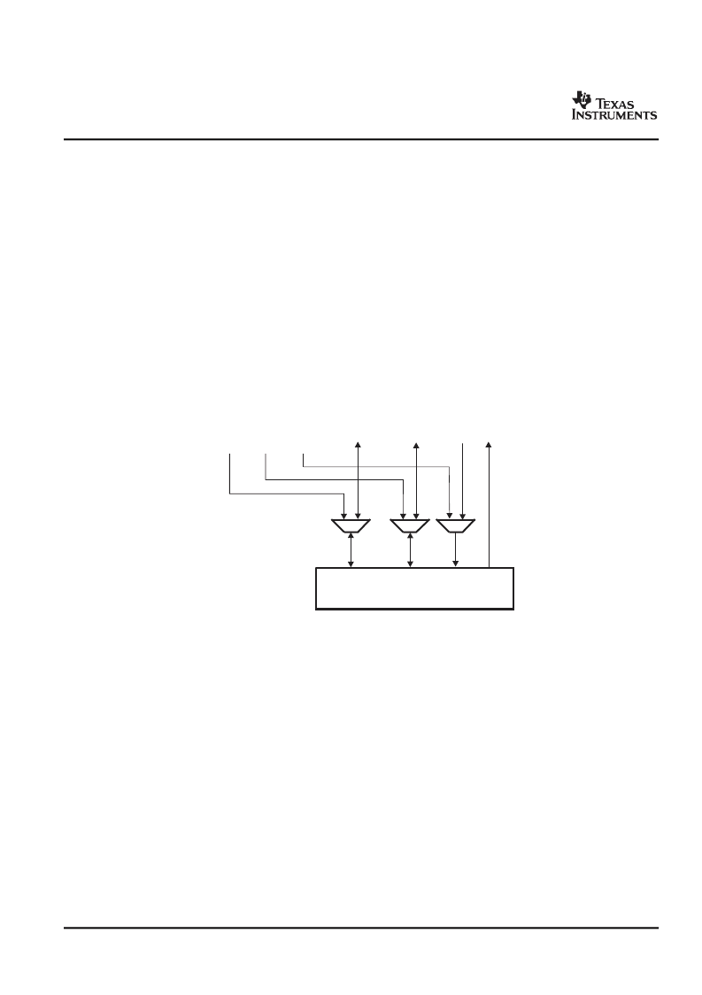
The data serial interface uses two sets of pins for communication between external devices, with the particular
pin used controlled through register programming. This configuration is shown in
Figure 18
below.
Figure 18. Alternate Audio Bus Mulitplexing Function
In cases where MFP3 is needed for a secondary device digital input, the TLV320AIC3106 must be used in I
2
C
mode (when in SPI mode, MFP3 is used as the SPI bus MOSI pin and thus cannot be used here as an alternate
digital input source).
This mux capability allows the TLV320AIC3106 to communicate with two separate devices with independent
I
2
S/PCM buses. An example of such an application is a cellphone containing a Bluetooth transceiver with
PCM/I
2
S interface, as shown in
Figure 19
. The applications processor can be connected to the WCLK, BCLK,
DIN, DOUT pins on the TLV320AIC3106, while a Bluetooth device with PCM interface can be connected to the
GPIO1, GPIO2, MFP3, and DOUT pins on the TLV320AIC3106. By programming the registers via I
2
C control,
the applications processor can determine which device is communicating with the TLV320AIC3106. This is
attractive in cases where the TLV320AIC3106 can be configured to communicate data with the Bluetooth device,
then the applications processor can be put into a low power sleep mode, while voice/audio transmission still
occurs between the Bluetooth device and the TLV320AIC3106.
22
Submit Documentation Feedback
相關(guān)PDF資料 |
PDF描述 |
|---|---|
| TLV320AIC3106IGQE | LOW-POWER STEREO AUDIO CODEC FOR PORTABLE AUDIO/TELEPHONY |
| TLV320AIC3106IGQER | LOW-POWER STEREO AUDIO CODEC FOR PORTABLE AUDIO/TELEPHONY |
| TLV341_07 | LOW-VOLTAGE RAIL-TO-RAIL OUTPUT CMOS OPERATIONAL AMPLIFLERS WITH SHUTDOWN |
| TLV431ACDBV | LOW-VOLTAGE ADJUSTABLE PRECISION SHUNT REGULATORS |
| TLV431ID | LOW-VOLTAGE ADJUSTABLE PRECISION SHUNT REGULATORS |
相關(guān)代理商/技術(shù)參數(shù) |
參數(shù)描述 |
|---|---|
| TLV320AIC3106EVM | 功能描述:音頻 IC 開發(fā)工具 TLV320AIC3106 Eval Mod RoHS:否 制造商:Texas Instruments 產(chǎn)品:Evaluation Kits 類型:Audio Amplifiers 工具用于評估:TAS5614L 工作電源電壓:12 V to 38 V |
| TLV320AIC3106EVM-K | 功能描述:音頻 IC 開發(fā)工具 TLV320AIC3106EVM-K Eval Mod RoHS:否 制造商:Texas Instruments 產(chǎn)品:Evaluation Kits 類型:Audio Amplifiers 工具用于評估:TAS5614L 工作電源電壓:12 V to 38 V |
| TLV320AIC3106IGQE | 制造商:Texas Instruments 功能描述:AUD CODEC 2ADC / 2DAC 24BIT 80BGA - Trays |
| TLV320AIC3106IGQER | 制造商:Texas Instruments 功能描述:AUD CODEC 2ADC / 2DAC 24BIT 80BGA - Tape and Reel |
| TLV320AIC3106IRGZR | 功能描述:接口—CODEC Lo-Pwr Stereo CODEC RoHS:否 制造商:Texas Instruments 類型: 分辨率: 轉(zhuǎn)換速率:48 kSPs 接口類型:I2C ADC 數(shù)量:2 DAC 數(shù)量:4 工作電源電壓:1.8 V, 2.1 V, 2.3 V to 5.5 V 最大工作溫度:+ 85 C 安裝風格:SMD/SMT 封裝 / 箱體:DSBGA-81 封裝:Reel |
發(fā)布緊急采購,3分鐘左右您將得到回復。