- 您現(xiàn)在的位置:買賣IC網(wǎng) > PDF目錄371186 > TLIU04C1 TLIU04C1 Quad T1/E1 Line Interface PDF資料下載
參數(shù)資料
| 型號(hào): | TLIU04C1 |
| 英文描述: | TLIU04C1 Quad T1/E1 Line Interface |
| 中文描述: | TLIU04C1四T1/E1線路接口 |
| 文件頁數(shù): | 49/100頁 |
| 文件大小: | 1321K |
| 代理商: | TLIU04C1 |
第1頁第2頁第3頁第4頁第5頁第6頁第7頁第8頁第9頁第10頁第11頁第12頁第13頁第14頁第15頁第16頁第17頁第18頁第19頁第20頁第21頁第22頁第23頁第24頁第25頁第26頁第27頁第28頁第29頁第30頁第31頁第32頁第33頁第34頁第35頁第36頁第37頁第38頁第39頁第40頁第41頁第42頁第43頁第44頁第45頁第46頁第47頁第48頁當(dāng)前第49頁第50頁第51頁第52頁第53頁第54頁第55頁第56頁第57頁第58頁第59頁第60頁第61頁第62頁第63頁第64頁第65頁第66頁第67頁第68頁第69頁第70頁第71頁第72頁第73頁第74頁第75頁第76頁第77頁第78頁第79頁第80頁第81頁第82頁第83頁第84頁第85頁第86頁第87頁第88頁第89頁第90頁第91頁第92頁第93頁第94頁第95頁第96頁第97頁第98頁第99頁第100頁
Advance Data Sheet, Rev. 2
April 1999
TLIU04C1 Quad T1/E1 Line Interface
49
Lucent Technologies Inc.
Microprocessor Mode
(continued)
XCLK Reference Clock
(continued)
Primary Line Rate XCLK Reference Clock and Internal Reference Clock Synthesizer
In some applications, it is more desirable to provide a reference clock at the primary data rate. In such cases, the
LIU can utilize an internal 16x clock synthesizer allowing the XCLK pin to accept a primary data rate clock. The
specifications for XCLK using a primary rate reference clock are defined in Table 29.
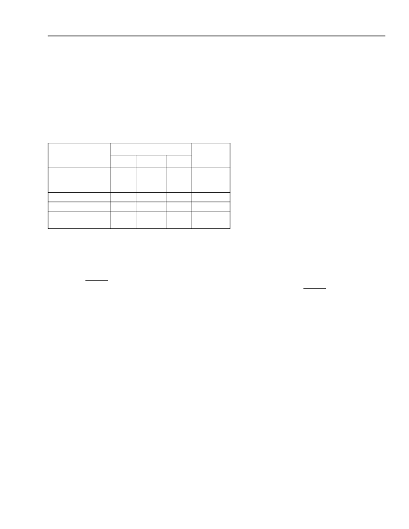
Table 29. XCLK (1x, CLKS = 1) Timing Specifications
* When JABW0 = 1 and the jitter attenuator is used in the receive data path, the tolerance on XCLK should be tightened to ±20 ppm in order to
meet the jitter accommodation requirements of TBR12/13 as given in G.823 for line data rates of ±50 ppm.
If XCLK is used as the source for AIS (see Alarm Indication Signal Generator (XAIS) on page 30), it must meet the nominal transmission
specifications of 1.544 MHz ± 32 ppm for DS1 (T1) or 2.048 MHz ± 50 ppm for CEPT (E1).
The data rate reference clock and the internal clock synthesizer are selected when CLKS = 1. In this mode, a valid
and stable data rate reference clock must be applied to the XCLK pin before and during the time a hardware reset
is activated (RESET = 0). The reset must be held active for a minimum of two data rate clock periods to ensure
proper resetting of the clock synthesizer circuit. Upon the deactivation of the reset pin (RESET = 1), the LIU will
extend the reset condition internally for approximately 1/2(2
12
– 1) line clock periods, or 1.3 ms for DS1 and
1 ms for CEPT after the hardware reset pin has become inactive, allowing the clock synthesizer additional time to
settle. No activity such as microprocessor read/write should be performed during this period. The device will be
operational 2.7 ms after the deactivation of the hardware reset pin. Issuing an LIU software restart (LIU_REG2
bit 5 (RESTART) = 1) does not impact the clock synthesizer circuit.
Power Supply Bypassing
External bypassing is required for all channels. A 1.0 μF capacitor must be connected between V
DDX
and GND
X
. In
addition, a 0.1 μF capacitor must be connected between V
DDD
and GND
D
, and a 0.1 μF capacitor must be con-
nected between V
DDA
and GND
A
. Ground plane connections are required for GND
X
, GND
D
, and GND
A
. Power
plane connections are also required for V
DDX
and V
DDD
. The need to reduce high-frequency coupling into the ana-
log supply (V
DDA
) may require an inductive bead to be inserted between the power plane and the V
DDA
pin of every
channel.
Capacitors used for power supply bypassing should be placed as close as possible to the device pins for maximum
effectiveness.
Parameter
Value
Unit
Min
Typ
Max
Frequency:
DS1
CEPT
Range*,
Duty Cycle
Rise and Fall Times
(10%—90%)
—
—
1.544
2.048
—
—
—
—
—
100
60
5
MHz
MHz
ppm
%
ns
–100
40
—
相關(guān)PDF資料 |
PDF描述 |
|---|---|
| TLIU04C1 | Quad T1/E1 Line Interface(四T1/E1線接口) |
| TLV3011AIDBVR | Nanopower, 1.8V, SOT23 Comparator with Voltage Reference |
| TLV349x | CAPACITOR, CLASS Y2 1.0NFCAPACITOR, CLASS Y2 1.0NF; Capacitance:1nF; Voltage rating, AC:250V; Voltage rating, DC:2500V; Capacitor dielectric type:Polypropylene; Series:B81122; Tolerance, +:20%; Tolerance, -:20%; Temp, op. |
| TLV3011AIDBVT | Nanopower, 1.8V, SOT23 Comparator with Voltage Reference |
| TLV3011AIDCKR | Nanopower, 1.8V, SOT23 Comparator with Voltage Reference |
相關(guān)代理商/技術(shù)參數(shù) |
參數(shù)描述 |
|---|---|
| TLIXF30001 | 制造商:GIGA 功能描述: |
| TLIXF30003 | 制造商:Rochester Electronics LLC 功能描述:- Bulk |
| TLIXF30007-852838 | 制造商:Cortina Systems Inc 功能描述: |
| TLIXF30009-865852 | 功能描述:IC OPT TRANSPORT PROC 868-TBGA RoHS:是 類別:集成電路 (IC) >> 接口 - 電信 系列:- 產(chǎn)品培訓(xùn)模塊:Lead (SnPb) Finish for COTS 產(chǎn)品變化通告:Product Discontinuation 06/Feb/2012 標(biāo)準(zhǔn)包裝:750 系列:* |
| TLIXF30010 | 制造商:Intel 功能描述: |
發(fā)布緊急采購,3分鐘左右您將得到回復(fù)。