- 您現(xiàn)在的位置:買賣IC網(wǎng) > PDF目錄384004 > TLC27L1BID (Texas Instruments, Inc.) LinCMOSE LOW-POWER OPERATIONAL AMPLIFIERS PDF資料下載
參數(shù)資料
| 型號(hào): | TLC27L1BID |
| 廠商: | Texas Instruments, Inc. |
| 英文描述: | LinCMOSE LOW-POWER OPERATIONAL AMPLIFIERS |
| 中文描述: | LinCMOSE低功耗運(yùn)算放大器 |
| 文件頁(yè)數(shù): | 27/33頁(yè) |
| 文件大小: | 538K |
| 代理商: | TLC27L1BID |
第1頁(yè)第2頁(yè)第3頁(yè)第4頁(yè)第5頁(yè)第6頁(yè)第7頁(yè)第8頁(yè)第9頁(yè)第10頁(yè)第11頁(yè)第12頁(yè)第13頁(yè)第14頁(yè)第15頁(yè)第16頁(yè)第17頁(yè)第18頁(yè)第19頁(yè)第20頁(yè)第21頁(yè)第22頁(yè)第23頁(yè)第24頁(yè)第25頁(yè)第26頁(yè)當(dāng)前第27頁(yè)第28頁(yè)第29頁(yè)第30頁(yè)第31頁(yè)第32頁(yè)第33頁(yè)
TLC27L2, TLC27L2A, TLC27L2B, TLC27L7
LinCMOS
PRECISION DUAL OPERATIONAL AMPLIFIERS
SLOS052B – OCTOBER 1987 – REVISED AUGUST 1994
27
POST OFFICE BOX 655303
DALLAS, TEXAS 75265
APPLICATION INFORMATION
input characteristics
The TLC27L2 and TLC27L7 are specified with a minimum and a maximum input voltage that, if exceeded at
either input, could cause the device to malfunction. Exceeding this specified range is a common problem,
especially in single-supply operation. Note that the lower range limit includes the negative rail, while the upper
range limit is specified at V
DD
–1 V at T
A
= 25
°
C and at V
DD
–1.5 V at all other temperatures.
The use of the polysilicon-gate process and the careful input circuit design gives the TLC27L2 and TLC27L7
very good input offset voltage drift characteristics relative to conventional metal-gate processes. Offset voltage
drift in CMOS devices is highly influenced by threshold voltage shifts caused by polarization of the phosphorus
dopant implanted in the oxide. Placing the phosphorus dopant in a conductor (such as a polysilicon gate)
alleviates the polarization problem, thus reducing threshold voltage shifts by more than an order of magnitude.
The offset voltage drift with time has been calculated to be typically 0.1
μ
V/month, including the first month of
operation.
Because of the extremely high input impedance and resulting low bias current requirements, the TLC27L2 and
TLC27L7 are well suited for low-level signal processing; however, leakage currents on printed circuit boards
and sockets can easily exceed bias current requirements and cause a degradation in device performance. It
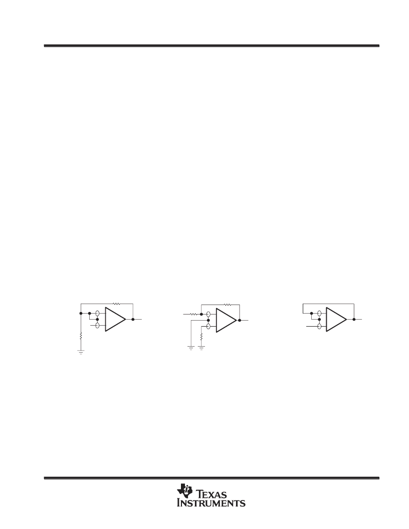
is good practice to include guard rings around inputs (similar to those of Figure 4 in the Parameter Measurement
Information section). These guards should be driven from a low-impedance source at the same voltage level
as the common-mode input (see Figure 40).
Unused amplifiers should be connected as grounded unity-gain followers to avoid possible oscillation.
noise performance
The noise specifications in operational amplifier circuits are greatly dependent on the current in the first-stage
differential amplifier. The low input bias current requirements of the TLC27L2 and TLC27L7 result in a very low
noise current, which is insignificant in most applications. This feature makes the devices especially favorable
over bipolar devices when using values of circuit impedance greater than 50 k
, since bipolar devices exhibit
greater noise currents.
VI
–
+
–
+
VI
(b) INVERTING AMPLIFIER
–
+
(c) UNITY-GAIN AMPLIFIER
(a) NONINVERTING AMPLIFIER
VI
VO
VO
VO
Figure 40. Guard-Ring Schemes
output characteristics
The output stage of the TLC27L2 and TLC27L7 is designed to sink and source relatively high amounts of current
(see typical characteristics). If the output is subjected to a short-circuit condition, this high current capability can
cause device damage under certain conditions. Output current capability increases with supply voltage.
All operating characteristics of the TLC27L2 and TLC27L7 were measured using a 20-pF load. The devices
drive higher capacitive loads; however, as output load capacitance increases, the resulting response pole
occurs at lower frequencies, thereby causing ringing, peaking, or even oscillation (see Figure 41). In many
cases, adding a small amount of resistance in series with the load capacitance alleviates the problem.
相關(guān)PDF資料 |
PDF描述 |
|---|---|
| TLC27L1BIP | LinCMOSE LOW-POWER OPERATIONAL AMPLIFIERS |
| TLC27L1ACD | LinCMOSE LOW-POWER OPERATIONAL AMPLIFIERS |
| TLC27L1AIP | LinCMOSE LOW-POWER OPERATIONAL AMPLIFIERS |
| TLC271MD | LinCMOSE PROGRAMMABLE LOW-POWER OPERATIONAL AMPLIFIERS |
| TLC271MFK | LinCMOSE PROGRAMMABLE LOW-POWER OPERATIONAL AMPLIFIERS |
相關(guān)代理商/技術(shù)參數(shù) |
參數(shù)描述 |
|---|---|
| TLC27L1BIP | 制造商:Rochester Electronics LLC 功能描述:- Bulk 制造商:Texas Instruments 功能描述: |
| TLC27L1CD | 功能描述:運(yùn)算放大器 - 運(yùn)放 LinCMOS Lo-Power Op Amp RoHS:否 制造商:STMicroelectronics 通道數(shù)量:4 共模抑制比(最小值):63 dB 輸入補(bǔ)償電壓:1 mV 輸入偏流(最大值):10 pA 工作電源電壓:2.7 V to 5.5 V 安裝風(fēng)格:SMD/SMT 封裝 / 箱體:QFN-16 轉(zhuǎn)換速度:0.89 V/us 關(guān)閉:No 輸出電流:55 mA 最大工作溫度:+ 125 C 封裝:Reel |
| TLC27L1CDG4 | 功能描述:運(yùn)算放大器 - 運(yùn)放 LinCMOS LO-PWR OP AMP RoHS:否 制造商:STMicroelectronics 通道數(shù)量:4 共模抑制比(最小值):63 dB 輸入補(bǔ)償電壓:1 mV 輸入偏流(最大值):10 pA 工作電源電壓:2.7 V to 5.5 V 安裝風(fēng)格:SMD/SMT 封裝 / 箱體:QFN-16 轉(zhuǎn)換速度:0.89 V/us 關(guān)閉:No 輸出電流:55 mA 最大工作溫度:+ 125 C 封裝:Reel |
| TLC27L1CDR | 功能描述:運(yùn)算放大器 - 運(yùn)放 LinCMOS Lo-Power Op Amp RoHS:否 制造商:STMicroelectronics 通道數(shù)量:4 共模抑制比(最小值):63 dB 輸入補(bǔ)償電壓:1 mV 輸入偏流(最大值):10 pA 工作電源電壓:2.7 V to 5.5 V 安裝風(fēng)格:SMD/SMT 封裝 / 箱體:QFN-16 轉(zhuǎn)換速度:0.89 V/us 關(guān)閉:No 輸出電流:55 mA 最大工作溫度:+ 125 C 封裝:Reel |
| TLC27L1CDRG4 | 功能描述:運(yùn)算放大器 - 運(yùn)放 LinCMOS Lo-Power Op Amp RoHS:否 制造商:STMicroelectronics 通道數(shù)量:4 共模抑制比(最小值):63 dB 輸入補(bǔ)償電壓:1 mV 輸入偏流(最大值):10 pA 工作電源電壓:2.7 V to 5.5 V 安裝風(fēng)格:SMD/SMT 封裝 / 箱體:QFN-16 轉(zhuǎn)換速度:0.89 V/us 關(guān)閉:No 輸出電流:55 mA 最大工作溫度:+ 125 C 封裝:Reel |
發(fā)布緊急采購(gòu),3分鐘左右您將得到回復(fù)。