- 您現(xiàn)在的位置:買賣IC網(wǎng) > PDF目錄383952 > TLC2254MFK (Texas Instruments, Inc.) Advanced LinCMOSE RAIL-TO-RAIL VERY LOW-POWER OPERATIONAL AMPLIFIERS PDF資料下載
參數(shù)資料
| 型號: | TLC2254MFK |
| 廠商: | Texas Instruments, Inc. |
| 元件分類: | 運動控制電子 |
| 英文描述: | Advanced LinCMOSE RAIL-TO-RAIL VERY LOW-POWER OPERATIONAL AMPLIFIERS |
| 中文描述: | 高級LinCMOSE軌至軌極低功耗運算放大器 |
| 文件頁數(shù): | 5/57頁 |
| 文件大小: | 926K |
| 代理商: | TLC2254MFK |
第1頁第2頁第3頁第4頁當前第5頁第6頁第7頁第8頁第9頁第10頁第11頁第12頁第13頁第14頁第15頁第16頁第17頁第18頁第19頁第20頁第21頁第22頁第23頁第24頁第25頁第26頁第27頁第28頁第29頁第30頁第31頁第32頁第33頁第34頁第35頁第36頁第37頁第38頁第39頁第40頁第41頁第42頁第43頁第44頁第45頁第46頁第47頁第48頁第49頁第50頁第51頁第52頁第53頁第54頁第55頁第56頁第57頁
TLC225x, TLC225xA
Advanced LinCMOS
RAIL-TO-RAIL
VERY LOW-POWER OPERATIONAL AMPLIFIERS
SLOS176A – FEBRUARY 1997 – REVISED JULY 1999
5
POST OFFICE BOX 655303
DALLAS, TEXAS 75265
absolute maximum ratings over operating free-air temperature range (unless otherwise noted)
Supply voltage, V
DD+
(see Note 1)
Supply voltage, V
DD–
(see Note 1)
Differential input voltage, V
ID
(see Note 2)
Input voltage, V
I
(any input, see Note 1)
Input current, I
I
(each input)
Output current, I
O
. . . . . . . . . . . . . . . . . . . . . . . . . . . . . . . . . . . . . . . . . . . . . . . . . . . . . . . . . . . . . . . . . . . . . . .
Total current into V
DD+
. . . . . . . . . . . . . . . . . . . . . . . . . . . . . . . . . . . . . . . . . . . . . . . . . . . . . . . . . . . . . . . . . .
Total current out of V
DD–
. . . . . . . . . . . . . . . . . . . . . . . . . . . . . . . . . . . . . . . . . . . . . . . . . . . . . . . . . . . . . . . .
Duration of short-circuit current at (or below) 25
°
C (see Note 3)
Continuous total dissipation
. . . . . . . . . . . . . . . . . . . . . . . . . . . . . . . . . . . . . . . . . . .
Operating free-air temperature range, T
A
: C suffix
I suffix
Q suffix
M suffix
Storage temperature range, T
stg
. . . . . . . . . . . . . . . . . . . . . . . . . . . . . . . . . . . . . . . . . . . . . . . . . . .
Lead temperature 1,6 mm (1/16 inch) from case for 10 seconds
8 V
–8 V
±
16 V
±
8 V
±
5 mA
±
50 mA
±
50 mA
±
50 mA
unlimited
. . . . . . . . . . . . . . . . . . . . . . . . . . . . . . . . . . . . . . . . . . . . . . . . . . . . . . . . . . . .
. . . . . . . . . . . . . . . . . . . . . . . . . . . . . . . . . . . . . . . . . . . . . . . . . . . . . . . . . . .
. . . . . . . . . . . . . . . . . . . . . . . . . . . . . . . . . . . . . . . . . . . . . . . . . . .
. . . . . . . . . . . . . . . . . . . . . . . . . . . . . . . . . . . . . . . . . . . . . . . . . . . . . .
. . . . . . . . . . . . . . . . . . . . . . . . . . . . . . . . . . . . . . . . . . . . . . . . . . . . . . . . . . . . . . .
. . . . . . . . . . . . . . . . . . . . . . . . . . . . . .
See Dissipation Rating Table
. . . . . . . . . . . . . . . . . . . . . . . . . . . . . . . . . . . . . .
. . . . . . . . . . . . . . . . . . . . . . . . . . . . . . . . . . . . .
. . . . . . . . . . . . . . . . . . . . . . . . . . . . . . . . . . .
. . . . . . . . . . . . . . . . . . . . . . . . . . . . . . . . . .
0
°
C to 70
°
C
–40
°
C to 85
°
C
–40
°
C to 125
°
C
–55
°
C to 125
°
C
–65
°
C to 150
°
C
260
°
C
. . . . . . . . . . . . . . . . . . . . . . . . . . . . . . .
Stresses beyond those listed under “absolute maximum ratings” may cause permanent damage to the device. These are stress ratings only, and
functional operation of the device at these or any other conditions beyond those indicated under “recommended operating conditions” is not
implied. Exposure to absolute-maximum-rated conditions for extended periods may affect device reliability.
NOTES:
1. All voltage values, except differential voltages, are with respect to the midpoint between VDD+ and VDD –.
2. Differential voltages are at IN+ with respect to IN–. Excessive current flows when input is brought below VDD– – 0.3 V.
3. The output may be shorted to either supply. Temperature and/or supply voltages must be limited to ensure that the maximum
dissipation rating is not exceeded.
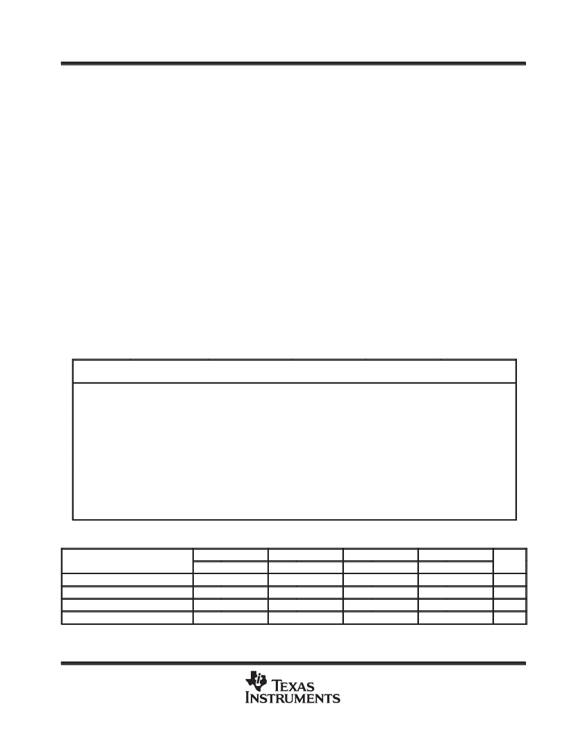
DISSIPATION RATING TABLE
PACKAGE
TA
≤
25
°
C
POWER RATING
DERATING FACTOR
ABOVE TA = 25
°
C
5.8 mW/
°
C
7.6 mW/
°
C
11.0 mW/
°
C
11.0 mW/
°
C
8.4 mW/
°
C
9.2 mW/
°
C
8.0 mW/
°
C
4.2 mW/
°
C
5.6 mW/
°
C
5.5 mW/
°
C
5.5 mW/
°
C
TA = 70
°
C
POWER RATING
TA = 85
°
C
POWER RATING
TA = 125
°
C
POWER RATING
D–8
724 mW
464 mW
377 mW
144 mW
D–14
950 mW
608 mW
450 mW
190 mW
FK
1375 mW
880 mW
715 mW
275 mW
J
1375 mW
880 mW
715 mW
275 mW
JG
1050 mW
672 mW
546 mW
275 mW
N
1150 mW
736 mW
736 mW
—
P
1000 mW
640 mW
520 mW
—
PW–8
525 mW
336 mW
273 mW
—
PW–14
700 mW
448 mW
448 mW
—
U
700 mW
246 mW
330 mW
150 mW
W
700 mW
246 mW
330 mW
150 mW
recommended operating conditions
C SUFFIX
I SUFFIX
Q SUFFIX
M SUFFIX
UNIT
MIN
±
2.2
VDD–
VDD–
MAX
±
8
VDD+ –1.5
VDD+ –1.5
70
MIN
±
2.2
VDD–
VDD–
–40
MAX
±
8
VDD+ –1.5
VDD+ –1.5
85
MIN
±
2.2
VDD–
VDD–
–40
MAX
±
8
VDD+ –1.5
VDD+ –1.5
125
MIN
±
2.2
VDD–
VDD–
–55
MAX
±
8
VDD+ –1.5
VDD+ –1.5
125
Supply voltage, VDD
±
Input voltage range, VI
Common-mode input voltage, VIC
Operating free-air temperature, TA
V
V
V
°
C
0
相關PDF資料 |
PDF描述 |
|---|---|
| TLC2252AMFK | TRANS ARRAY NPN/NPN W/RES MINI-6 |
| TLC2252AMJG | Advanced LinCMOSE RAIL-TO-RAIL VERY LOW-POWER OPERATIONAL AMPLIFIERS |
| TLC2252AMU | TRANS ARRAY PNP/PNP MINI-6P |
| TLC2252MJG | BEZEL FOR ZU-M2121 SERIES |
| TLC2252MU | Advanced LinCMOSE RAIL-TO-RAIL VERY LOW-POWER OPERATIONAL AMPLIFIERS |
相關代理商/技術參數(shù) |
參數(shù)描述 |
|---|---|
| TLC2254MFKB | 制造商:Texas Instruments 功能描述:OP Amp Quad GP R-R O/P 制造商:Rochester Electronics LLC 功能描述:- Bulk 制造商:Texas Instruments 功能描述:5962-9564002Q2A QUAD OP AMP |
| TLC2254MJ | 制造商:TI 制造商全稱:Texas Instruments 功能描述:Advanced LinCMOS RAIL-TO-RAIL VERY LOW-POWER OPERATIONAL AMPLIFIERS |
| TLC2254MJB | 制造商:TI 制造商全稱:Texas Instruments 功能描述:Advanced LinCMOS RAIL-TO-RAIL VERY LOW-POWER OPERATIONAL AMPLIFIERS |
| TLC2254MW | 制造商:TI 制造商全稱:Texas Instruments 功能描述:Advanced LinCMOSE RAIL-TO-RAIL VERY LOW-POWER OPERATIONAL AMPLIFIERS |
| TLC2254MWB | 制造商:TI 制造商全稱:Texas Instruments 功能描述:Advanced LinCMOS RAIL-TO-RAIL VERY LOW-POWER OPERATIONAL AMPLIFIERS |
發(fā)布緊急采購,3分鐘左右您將得到回復。