- 您現(xiàn)在的位置:買(mǎi)賣IC網(wǎng) > PDF目錄98234 > TLC1225IFNR (TEXAS INSTRUMENTS INC) 1-CH 12-BIT SUCCESSIVE APPROXIMATION ADC, PARALLEL ACCESS, PQCC28 PDF資料下載
參數(shù)資料
| 型號(hào): | TLC1225IFNR |
| 廠商: | TEXAS INSTRUMENTS INC |
| 元件分類: | ADC |
| 英文描述: | 1-CH 12-BIT SUCCESSIVE APPROXIMATION ADC, PARALLEL ACCESS, PQCC28 |
| 封裝: | PLASTIC, LCC-28 |
| 文件頁(yè)數(shù): | 1/15頁(yè) |
| 文件大小: | 230K |
| 代理商: | TLC1225IFNR |
當(dāng)前第1頁(yè)第2頁(yè)第3頁(yè)第4頁(yè)第5頁(yè)第6頁(yè)第7頁(yè)第8頁(yè)第9頁(yè)第10頁(yè)第11頁(yè)第12頁(yè)第13頁(yè)第14頁(yè)第15頁(yè)

TLC1225I, TLC1225M
SELF-CALIBRATING 12-BIT-PLUS-SIGN
ANALOG-TO-DIGITAL CONVERTERS
SLAS029B – AUGUST 1990 – REVISED DECEMBER 1993
Copyright
1993, Texas Instruments Incorporated
1
POST OFFICE BOX 655303
DALLAS, TEXAS 75265
Advanced LinCMOS Technology
Self Calibration Eliminates Expensive
Trimming at Factory and Offset Adjustment
in the Field
12-Bit-Plus-Sign Resolution
12-Bit Linearity
12-s Conversion Period at f
clock = 2 MHz
Compatible With All Microprocessors
Single 5-V and ±5-V Supply Operation
True Differential Analog Voltage Inputs
With – Vref to Vref Differential Input Range
For Single 5-V Supply, Input
Common-Mode Voltage Range is 0 V to 5 V
For ±5-V Supplies, Input Common-Mode
Voltage Range is – 5 V to 5 V
Unipolar or Bipolar Operation
2s-Complement Output
Low Power
85 mW Max on TLC1225I
87.5 mW Max on TLC1225M
description
The TLC1225I and TLC1225M converters are
manufactured with Texas Instruments highly
efficient Advanced LinCMOS
technology. The
TLC1225I and TLC1225M CMOS analog-to-
digital converters (ADCs) can be operated with a
single 5-V supply or with
±5-V supplies. The
differential input range is – Vref to Vref in both
supply configurations. The common-mode input
range is ANLG VCC– to ANLG VCC+. For single
5-V supply operation, grounding IN – corresponds
to standard unipolar conversion. For
±5-V supply
operation,
grounding
IN –
corresponds
to
standard
bipolar
conversion.
Conversion
is
performed
via
the successive-approximation
method. The TLC1225x outputs the converted data in a parallel word and interfaces directly to a 16-bit data bus.
Negative numbers are given in the 2s-complement data format. All digital signals are fully TTL and CMOS
compatible.
This converter uses a self-calibration technique by which seven of the internal capacitors in the capacitive array
of the A/D conversion circuitry can be automatically calibrated. The internal capacitors are calibrated during a
nonconversion capacitor-calibrate cycle in which all seven of the internal capacitors are calibrated at the same
time. A conversion period requires only 24 clock cycles. Self calibration requires 300 clock cycles. The
calibration or conversion cycle can be initiated at any time by issuing the proper command word to the data bus.
The self-calibrating technique eliminates the need for expensive trimming of thin-film resistors at the factory and
provides excellent performance at low cost.
Advanced LinCMOS is a trademark of Texas Instruments Incorporated.
The conversion period is the reciprocal of the conversion rate and includes the access, sample, setup, and A/D conversion times.
1
2
3
4
5
6
7
8
9
10
11
12
13
14
28
27
26
25
24
23
22
21
20
19
18
17
16
15
ANLG VCC–
IN –
IN +
ANLG GND
REF
ANLG VCC+
TIE HIGH
CLK IN
WR
CS
RD
DGTL GND
READY OUT
INT
DGTL VCC
D12
D11
D10
D9
D8
D7
D6
D5/D15
D4/D14
D3/D13
D2/D12
D1/D11
D0/D10
I/O
Bus
32 1
13 14
5
6
7
8
9
10
11
D10
D9
D8
D7
D6
D5/D15
D4/D14
REF
ANLG VCC+
TIE HIGH
CLK IN
WR
CS
RD
4
15 16 17 18
READY
OUT
INT
D0/D10
D1/D1
1
D2/D12
D3/D13
ANLG
GND
IN+
IN–
ANLG
V
28 27 26
25
24
23
22
21
20
19
12
DGTL
GND
DGTL
V
D12
D1
1
CC
–
CC
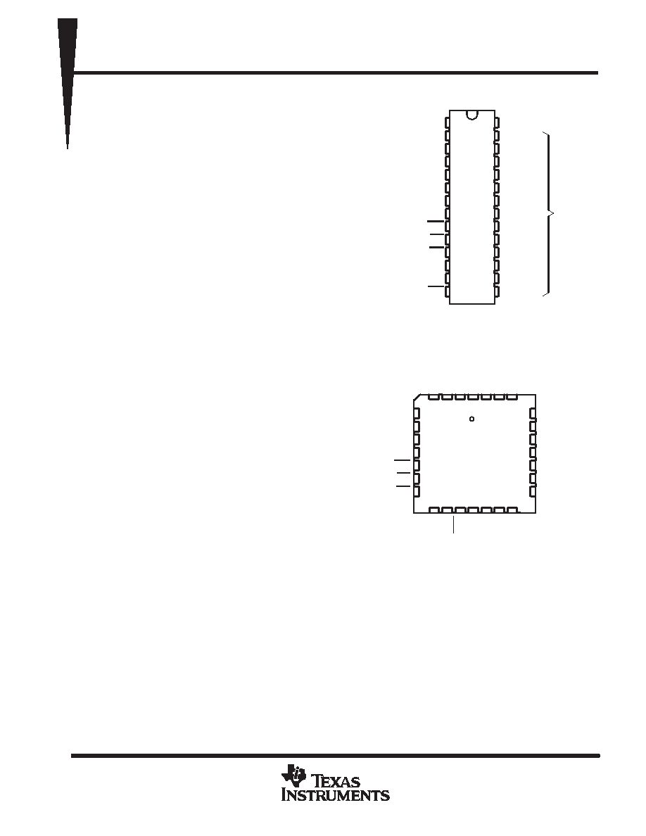
FK OR FN PACKAGE
(TOP VIEW)
J OR NW PACKAGE
(TOP VIEW)
PRODUCTION DATA information is current as of publication date.
Products conform to specifications per the terms of Texas Instruments
standard warranty. Production processing does not necessarily include
testing of all parameters.
相關(guān)PDF資料 |
PDF描述 |
|---|---|
| TLC1514IPWLE | 4-CH 10-BIT SUCCESSIVE APPROXIMATION ADC, SERIAL ACCESS, PDSO16 |
| TLC1518IPWLE | 8-CH 10-BIT SUCCESSIVE APPROXIMATION ADC, SERIAL ACCESS, PDSO20 |
| TLC1518IDWRG4 | 8-CH 10-BIT SUCCESSIVE APPROXIMATION ADC, SERIAL ACCESS, PDSO20 |
| TLC1514IDRG4 | 4-CH 10-BIT SUCCESSIVE APPROXIMATION ADC, SERIAL ACCESS, PDSO16 |
| TLC1518IDW | 8-CH 10-BIT SUCCESSIVE APPROXIMATION ADC, SERIAL ACCESS, PDSO20 |
相關(guān)代理商/技術(shù)參數(shù) |
參數(shù)描述 |
|---|---|
| TLC1225IN | 制造商:Rochester Electronics LLC 功能描述: 制造商:Texas Instruments 功能描述: |
| TLC1225MJB | 制造商:Rochester Electronics LLC 功能描述:- Bulk |
| TLC139 | 制造商:TI 制造商全稱:Texas Instruments 功能描述:LinCMOSE MICROPOWER QUAD COMPARATORS |
| TLC139D | 制造商:TI 制造商全稱:Texas Instruments 功能描述:LinCMOSE MICROPOWER QUAD COMPARATORS |
| TLC139FK | 制造商:TI 制造商全稱:Texas Instruments 功能描述:LinCMOSE MICROPOWER QUAD COMPARATORS |
發(fā)布緊急采購(gòu),3分鐘左右您將得到回復(fù)。