- 您現(xiàn)在的位置:買賣IC網(wǎng) > PDF目錄383951 > TL598D (Texas Instruments, Inc.) PULSE-WIDTH-MODULATION CONTROL CIRCUITS PDF資料下載
參數(shù)資料
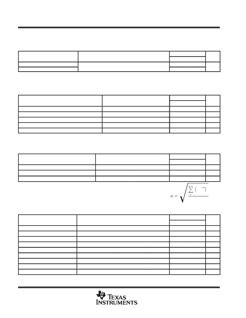
| 型號(hào): | TL598D |
| 廠商: | Texas Instruments, Inc. |
| 英文描述: | PULSE-WIDTH-MODULATION CONTROL CIRCUITS |
| 中文描述: | 脈寬調(diào)制控制電路 |
| 文件頁(yè)數(shù): | 6/10頁(yè) |
| 文件大?。?/td> | 154K |
| 代理商: | TL598D |
TL598
PULSE-WIDTH-MODULATION CONTROL CIRCUITS
SLVS053C – FEBRUARY 1988 – REVISED JULY 1999
6
POST OFFICE BOX 655303
DALLAS, TEXAS 75265
electrical characteristics over recommended operating free-air temperature range, V
CC
= 15 V
(unless otherwise noted)
switching characteristics, T
A
= 25
°
C
(see Note 4)
PARAMETER
TEST CONDITIONS
TL598C, TL598Q
MIN
TYP
UNIT
MAX
150
75
Output-voltage rise time
Output-voltage fall time
NOTE 4. Pulse-testing techniques must be used that maintain the junction temperature as close to the ambient temperature as possible.
CL = 1500 pF,
See Figure 2
VC = 15 V,
VCC = 15 V,
60
35
ns
electrical characteristics, V
CC
= 15 V, T
A
= 25
°
C
reference section (see Note 4)
PARAMETER
TEST CONDITIONS
TL598Y
TYP
UNIT
MIN
MAX
Output voltage (REF)
IO = 1 mA
VCC = 7 V to 40 V
IO = 1 mA to 10 mA
5
V
Input regulation
2
mV
Output regulation
1
mV
Output-voltage change with temperature
Short-circuit output current
All typical values except for parameter changes with temperature are at TA = 25
°
C.
Duration of the short circuit should not exceed one second.
NOTE 4. Pulse-testing techniques that maintain the junction temperature as close to the ambient temperature as possible must be used.
2
mV/V
REF = 0 V
–48
mA
oscillator section, C
T
= 0.001
μ
F, R
T
= 12 k
(see Figure 1) (see Note 4)
PARAMETER
TEST CONDITIONS
TL598Y
UNIT
MIN
TYP
100
MAX
Frequency
Standard deviation of frequency§
Frequency change with voltage
§Standard deviation is a measure of the statistical distribution about the mean as derived from the formula:
kHz
All values of VCC, CT, RT, TA constant
VCC = 7 V to 40 V,
100
Hz/kHz
1
Hz/kHz
N
n
1
x
n
–X
2
N–1
NOTE 4. Pulse-testing techniques that maintain the junction temperature as close to the ambient temperature as possible must be used.
error amplifier section (see Note 4)
PARAMETER
TEST CONDITIONS
TL598Y
TYP
UNIT
MIN
MAX
Input offset voltage
Feedback = 2.5 V
2
mV
Input offset current
Feedback = 2.5 V
25
nA
μ
A
dB
Input bias current
Feedback = 2.5 V
VO (FEEDBACK) = 3 V,
0.2
Open-loop voltage amplification
VO (FEEDBACK) = 0.5 V to 3.5 V
95
Unity-gain bandwidth
800
kHz
Common-mode rejection ratio
VCC = 40 V,
FEEDBACK = 0.5 V
VIC = 6.5 V,
80
dB
Output sink current (FEEDBACK)
0.7
65
°
100
mA
Phase margin at unity gain
FEEDBACK = 0.5 V to 3.5 V,
RL = 2 k
RL = 2 k
Supply-voltage rejection ratio
FEEDBACK = 2.5 V,
VCC = 33 V,
dB
NOTE 4. Pulse-testing techniques that maintain the junction temperature as close to the ambient temperature as possible must be used.
相關(guān)PDF資料 |
PDF描述 |
|---|---|
| TL598N | Expandable Sleeving |
| TL66 | TWIN-BOBBIN TRANSFORMER |
| TL66-12F-10 | TWIN-BOBBIN TRANSFORMER |
| TL66-12F-12 | TWIN-BOBBIN TRANSFORMER |
| TL66-12F-120 | TWIN-BOBBIN TRANSFORMER |
相關(guān)代理商/技術(shù)參數(shù) |
參數(shù)描述 |
|---|---|
| TL598MFKB | 制造商:TI 制造商全稱:Texas Instruments 功能描述:PULSE-WIDTH-MODULATION CONTROL CIRCUITS |
| TL598MJB | 制造商:TI 制造商全稱:Texas Instruments 功能描述:PULSE-WIDTH-MODULATION CONTROL CIRCUITS |
| TL598N | 制造商:TI 制造商全稱:Texas Instruments 功能描述:PULSE-WIDTH-MODULATION CONTROL CIRCUITS |
| TL598QD | 制造商:TI 制造商全稱:Texas Instruments 功能描述:PULSE-WIDTH-MODULATION CONTROL CIRCUITS |
| TL598QDR | 制造商:TI 制造商全稱:Texas Instruments 功能描述:PULSE-WIDTH-MODULATION CONTROL CIRCUITS |
發(fā)布緊急采購(gòu),3分鐘左右您將得到回復(fù)。