- 您現(xiàn)在的位置:買賣IC網(wǎng) > PDF目錄384001 > TL1454AY (Texas Instruments, Inc.) DUAL-CHANNEL PULSE-WIDTH-MODULATION (PWM) CONTROL CIRCUIT PDF資料下載
參數(shù)資料
| 型號: | TL1454AY |
| 廠商: | Texas Instruments, Inc. |
| 英文描述: | DUAL-CHANNEL PULSE-WIDTH-MODULATION (PWM) CONTROL CIRCUIT |
| 中文描述: | 雙通道脈寬調(diào)制(PWM)控制電路 |
| 文件頁數(shù): | 4/27頁 |
| 文件大?。?/td> | 409K |
| 代理商: | TL1454AY |
第1頁第2頁第3頁當前第4頁第5頁第6頁第7頁第8頁第9頁第10頁第11頁第12頁第13頁第14頁第15頁第16頁第17頁第18頁第19頁第20頁第21頁第22頁第23頁第24頁第25頁第26頁第27頁
TL1454A, TL1454AY
DUAL-CHANNEL PULSE-WIDTH-MODULATION (PWM)
CONTROL CIRCUIT
SLVS423 A
–
MAY 2002
–
REVISED SEPTEMBER 2002
4
POST OFFICE BOX 655303
DALLAS, TEXAS 75265
theory of operation
reference voltage
A linear regulator operating from V
CC
generates a 2.5-V supply for the internal circuits and the 1.26-V reference,
which can source a maximum of 1 mA for external loads. A small ceramic capacitor (0.047
μ
F to 0.1
μ
F) between
REF and ground is recommended to minimize noise pickup.
error amplifier
The error amplifier generates the error signal used by the PWM to adjust the power-switch duty cycle for the
desired converter output voltage. The signal is generated by comparing a sample of the output voltage to the
voltage reference and amplifying the difference. An external resistive divider connected between the converter
output and ground, as shown in Figure 1, is generally required to obtain the output voltage sample.
The amplifier output is brought out on COMP to allow the frequency response of the amplifier to be shaped with
an external RC network to stabilize the feedback loop of the converter. DC loading on the COMP output is limited
to 45
μ
A (the maximum amplifier source current capability).
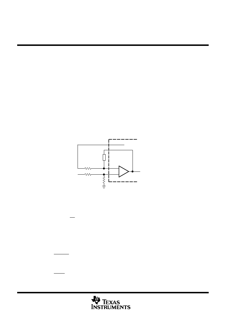
Figure 1 illustrates the sense-divider network and error-amplifier connections for converters with positive output
voltages. The divider network is connected to the noninverting amplifier input because the PWM has a phase
inversion; the duty cycle decreases as the error-amplifier output increases.
_
+
IN
–
IN+
R3
R1
R2
COMP
To PWM
VO
Compensation
Network
REF
Converter
Output
TL1454A
Figure 1. Sense Divider/Error Amplifier
Configuration for Converters with Positive Outputs
The output voltage is given by:
VO
Vref
1
R1
R2
where V
ref
= 1.26 V.
The dc source resistance of the error-amplifier inputs should be 10 k
or less and approximately matched to
minimize output voltage errors caused by the input-bias current. A simple procedure for determining appropriate
values for the resistors is to choose a convenient value for R3 (10 k
or less) and calculate R1 and R2 using:
R1
R3VO
VO
–
Vref
R2
R3VO
Vref
相關(guān)PDF資料 |
PDF描述 |
|---|---|
| TL1593CNS | 780- 】 488-pixel ccd image sensor |
| TL2575_08 | 1-A SIMPLE STEP-DOWN SWITCHING VOLTAGE REGULATORS |
| TL2575ADJI | 1-A SIMPLE STEP-DOWN SWITCHING VOLTAGE REGULATORS |
| TL2575HV | 1-A SIMPLE STEP-DOWN SWITCHING VOLTAGE REGULATORS |
| TL2575_07 | 1-A SIMPLE STEP-DOWN SWITCHING VOLTAGE REGULATORS |
相關(guān)代理商/技術(shù)參數(shù) |
參數(shù)描述 |
|---|---|
| TL1454CD | 制造商:Rochester Electronics LLC 功能描述:- Bulk |
| TL1454CDR | 制造商:Rochester Electronics LLC 功能描述:- Bulk |
| TL1454CN | 制造商:Rochester Electronics LLC 功能描述:- Bulk |
| TL1454CNSR | 制造商:Rochester Electronics LLC 功能描述:- Bulk |
| TL1454CPW | 制造商:TI 制造商全稱:Texas Instruments 功能描述:DUAL-CHANNEL PULSE-WIDTH-MODULATION (PWM) CONTROL CIRCUIT |
發(fā)布緊急采購,3分鐘左右您將得到回復(fù)。