- 您現(xiàn)在的位置:買賣IC網(wǎng) > PDF目錄384001 > TL052MP (Texas Instruments, Inc.) ENHANCED-JFET LOW-OFFSET OPERATIONAL AMPLIFIERS PDF資料下載
參數(shù)資料
| 型號: | TL052MP |
| 廠商: | Texas Instruments, Inc. |
| 英文描述: | ENHANCED-JFET LOW-OFFSET OPERATIONAL AMPLIFIERS |
| 中文描述: | 增強(qiáng)型場效應(yīng)低失調(diào)運(yùn)算放大器 |
| 文件頁數(shù): | 61/65頁 |
| 文件大小: | 1022K |
| 代理商: | TL052MP |
第1頁第2頁第3頁第4頁第5頁第6頁第7頁第8頁第9頁第10頁第11頁第12頁第13頁第14頁第15頁第16頁第17頁第18頁第19頁第20頁第21頁第22頁第23頁第24頁第25頁第26頁第27頁第28頁第29頁第30頁第31頁第32頁第33頁第34頁第35頁第36頁第37頁第38頁第39頁第40頁第41頁第42頁第43頁第44頁第45頁第46頁第47頁第48頁第49頁第50頁第51頁第52頁第53頁第54頁第55頁第56頁第57頁第58頁第59頁第60頁當(dāng)前第61頁第62頁第63頁第64頁第65頁
TL05x, TL05xA, TL05xY
ENHANCED-JFET LOW-OFFSET
OPERATIONAL AMPLIFIERS
SLOS178 – FEBRUARY 1997
61
POST OFFICE BOX 655303
DALLAS, TEXAS 75265
APPLICATION INFORMATION
voltage-ratio-to-dB converter
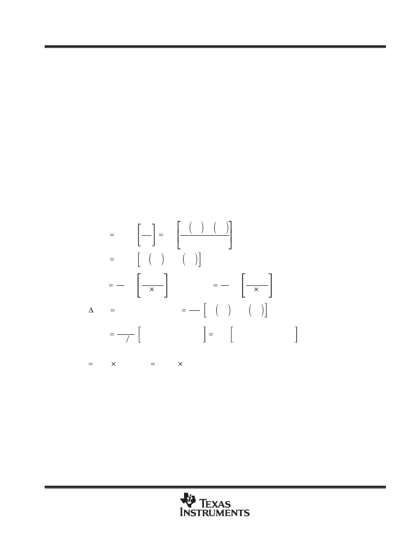
The application in Figure 90 measures the amplitude ratio of two signals and then converts the ratio to decibels
(see Figure 91). The output voltage provides a resolution of 100 mV/dB. The two inputs can be either dc or
sinusoidal ac signals. When using ac signals, both signals should be the same frequency or output glitches will
occur. For measuring two input signals of different frequencies, extra filtering should be added after the
rectifiers.
The circuit contains three low-offset TL05xA devices. Two of these devices provide the rectification and
logarithmic conversion of the inputs. The third TL05xA forms an instrumentation amplifier. The stage performing
the logarithmic conversion also requires two well-matched npn transistors.
The input signal first passes through a high impedance unity-gain buffer U1A (U2A). Then U1B (U2B) rectifies
the input signal at a gain of 0.5, and U1C (U2C) provides a noninverting gain of 2 so that the system gain is still
one. U1D (U2D), R6 (R13), and Q1 (Q2) perform the logarithmic conversion of the rectified input signal. The
instrumentation amplifier formed by U3A, U3B, U3D scales the difference of the two logarithmic voltages by a
gain of 33.6. As a result, the output voltage equals 100 mV/dB. The 1-k
potentiometer on the input of U3C
calibrates the zero dB reference level. The following equations are used to derive the relationship between the
input voltage ratio expressed in decibels and the output voltage.
X dB
20 log
VA
VB
20
In VA
– VB
In (10)
X dB
8.686 In VA
– In VB
VBE(Q1)
kT
q
In
VA
R
IS
VBE(Q2)
kT
q
In
VB
R
IS
VBE
VBE(Q1)–VBE(Q2)
kT
q
In VA
– In VB
X dB
8.686
kT q
VBE(Q1)–VBE(Q2)
336
VBE(Q1)–VBE(Q2)
at 25
°
C
where
k
1.38
10–23, q
1.602
10–19, and T is in kelvins.
This would give a resolution of 1 V/dB. Therefore, the gain of the instrumentation amplifier is set at 33.6 to obtain
100 mV/dB.
相關(guān)PDF資料 |
PDF描述 |
|---|---|
| TL052Y | ENHANCED-JFET LOW-OFFSET OPERATIONAL AMPLIFIERS |
| TL054ACD | ENHANCED-JFET LOW-OFFSET OPERATIONAL AMPLIFIERS |
| TL054MD | ENHANCED-JFET LOW-OFFSET OPERATIONAL AMPLIFIERS |
| TL054MN | Electrical, Duct/Raceway (Trunking); |
| TL054Y | ENHANCED-JFET LOW-OFFSET OPERATIONAL AMPLIFIERS |
相關(guān)代理商/技術(shù)參數(shù) |
參數(shù)描述 |
|---|---|
| TL052Y | 制造商:TI 制造商全稱:Texas Instruments 功能描述:ENHANCED-JFET LOW-OFFSET OPERATIONAL AMPLIFIERS |
| TL054 | 制造商:TI 制造商全稱:Texas Instruments 功能描述:ENHANCED-JFET LOW-OFFSET OPERATIONAL AMPLIFIERS |
| TL054ACD | 功能描述:運(yùn)算放大器 - 運(yùn)放 Enhanced Prec D RoHS:否 制造商:STMicroelectronics 通道數(shù)量:4 共模抑制比(最小值):63 dB 輸入補(bǔ)償電壓:1 mV 輸入偏流(最大值):10 pA 工作電源電壓:2.7 V to 5.5 V 安裝風(fēng)格:SMD/SMT 封裝 / 箱體:QFN-16 轉(zhuǎn)換速度:0.89 V/us 關(guān)閉:No 輸出電流:55 mA 最大工作溫度:+ 125 C 封裝:Reel |
| TL054ACDE4 | 功能描述:運(yùn)算放大器 - 運(yùn)放 Enhanced-JFET Precision Quad RoHS:否 制造商:STMicroelectronics 通道數(shù)量:4 共模抑制比(最小值):63 dB 輸入補(bǔ)償電壓:1 mV 輸入偏流(最大值):10 pA 工作電源電壓:2.7 V to 5.5 V 安裝風(fēng)格:SMD/SMT 封裝 / 箱體:QFN-16 轉(zhuǎn)換速度:0.89 V/us 關(guān)閉:No 輸出電流:55 mA 最大工作溫度:+ 125 C 封裝:Reel |
| TL054ACDG4 | 功能描述:運(yùn)算放大器 - 運(yùn)放 Enh-JFET Prec Quad Op Amp RoHS:否 制造商:STMicroelectronics 通道數(shù)量:4 共模抑制比(最小值):63 dB 輸入補(bǔ)償電壓:1 mV 輸入偏流(最大值):10 pA 工作電源電壓:2.7 V to 5.5 V 安裝風(fēng)格:SMD/SMT 封裝 / 箱體:QFN-16 轉(zhuǎn)換速度:0.89 V/us 關(guān)閉:No 輸出電流:55 mA 最大工作溫度:+ 125 C 封裝:Reel |
發(fā)布緊急采購,3分鐘左右您將得到回復(fù)。