- 您現(xiàn)在的位置:買賣IC網 > PDF目錄384001 > TL052MD (Texas Instruments, Inc.) ENHANCED-JFET LOW-OFFSET OPERATIONAL AMPLIFIERS PDF資料下載
參數(shù)資料
| 型號: | TL052MD |
| 廠商: | Texas Instruments, Inc. |
| 英文描述: | ENHANCED-JFET LOW-OFFSET OPERATIONAL AMPLIFIERS |
| 中文描述: | 增強型場效應低失調運算放大器 |
| 文件頁數(shù): | 10/65頁 |
| 文件大?。?/td> | 1022K |
| 代理商: | TL052MD |
第1頁第2頁第3頁第4頁第5頁第6頁第7頁第8頁第9頁當前第10頁第11頁第12頁第13頁第14頁第15頁第16頁第17頁第18頁第19頁第20頁第21頁第22頁第23頁第24頁第25頁第26頁第27頁第28頁第29頁第30頁第31頁第32頁第33頁第34頁第35頁第36頁第37頁第38頁第39頁第40頁第41頁第42頁第43頁第44頁第45頁第46頁第47頁第48頁第49頁第50頁第51頁第52頁第53頁第54頁第55頁第56頁第57頁第58頁第59頁第60頁第61頁第62頁第63頁第64頁第65頁
TL05x, TL05xA, TL05xY
ENHANCED-JFET LOW-OFFSET
OPERATIONAL AMPLIFIERS
SLOS178 – FEBRUARY 1997
10
POST OFFICE BOX 655303
DALLAS, TEXAS 75265
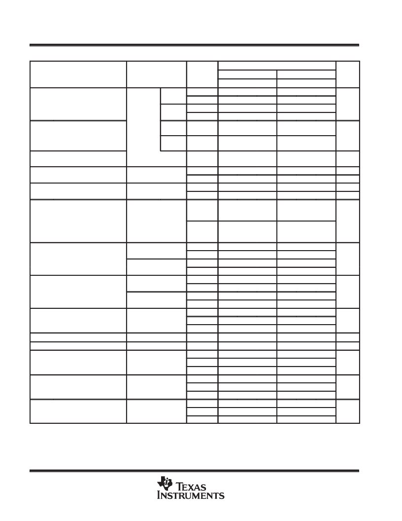
TL051I and TL051AI electrical characteristics at specified free-air temperature
TL051I, TL051AI
PARAMETER
TEST CONDITIONS
TA
VCC
±
=
±
5 V
MIN
VCC
±
=
±
15 V
MIN
TYP
0.59
UNIT
TYP
0.75
MAX
3.5
5.3
2.8
4.6
MAX
1.5
3.3
0.8
2.6
TL051I
25
°
C
VIO
Input offset voltage
Full range
25
°
C
Full range
25
°
C to
85
°
C
25
°
C to
85
°
C
mV
TL051AI
0.55
0.35
VO= 0
VO = 0,
VIC = 0,
RS = 50
VIO
α
Temperature coefficient of
input offset voltage
TL051I
7
8
μ
V/
°
C
TL051AI
8
8
25
Input offset voltage
long-term drift§
25
°
C
0.04
0.04
μ
V/mo
IIO
Input offset current
VO = 0,
See Figure 5
VIC = 0,
25
°
C
85
°
C
25
°
C
85
°
C
4
100
10
200
20
5
100
10
200
20
pA
nA
pA
nA
0.06
20
0.6
–2.3
0.07
30
0.7
–12.3
IIB
Input bias current
VO = 0,
See Figure 5
VIC = 0,
VICR
Common-mode input
voltage range
25
°
C
–1
to
4
to
5.6
–11
to
11
to
15.6
V
Full range
–1
to
4
3
3
–11
to
11
13
13
RL= 10 k
RL = 10 k
25
°
C
4.2
13.9
VOM +
Maximum positive peak
output voltage swing
Full range
25
°
C
Full range
25
°
C
Full range
25
°
C
Full range
25
°
C
–40
°
C
85
°
C
25
°
C
25
°
C
25
°
C
–40
°
C
85
°
C
25
°
C
–40
°
C
85
°
C
25
°
C
–40
°
C
85
°
C
V
RL= 2 k
RL = 2 k
2.5
2.5
–2.5
–2.5
–2.3
–2.3
25
30
20
3.8
11.5
11.5
–12
–12
–11
–11
50
60
30
12.7
RL= 10 k
RL = 10 k
–3.5
–13.2
VOM –
Maximum negative peak
output voltage swing
V
RL= 2 k
RL = 2 k
–3.2
–12
Large signal differential
Large-signal differential
voltage amplification
voltage am lification
59
74
43
105
145
76
1012
12
93
90
93
99
98
99
2.7
2.6
2.6
AVD
RL = 2 k
V/mV
ri
ci
Input resistance
Input capacitance
1012
10
85
83
84
99
98
99
2.6
2.4
2.5
pF
Common mode
Common-mode
rejection ratio
VIC = VICRmin,
VIC VICRmin,
VO = 0,
RS = 50
65
65
65
75
75
75
75
75
75
75
75
75
CMRR
dB
Supply voltage rejection
Supply-voltage rejection
VO = 0,
RS= 50
RS = 50
kSVR
dB
ratio (
VCC
±
/
VIO)
3.2
3.2
3.2
3.2
3.2
3.2
ICC
Supply current
VO = 0,
No load
mA
Full range is –40
°
C to 85
°
C
This parameter is tested on a sample basis for the TL051A. For other test requirements, please contact the factory. This statement has no bearing
on testing or nontesting of other parameters.
§Typical values are based on the input offset voltage shift observed through 168 hours of operating life test at TA = 150
°
C extrapolated to
TA = 25
°
C using the Arrhenius equation and assuming an activation energy of 0.96 eV.
For VCC
±
=
±
5 V, VO =
±
2.3 V, or for VCC
±
=
±
15 V, VO =
±
10 V.
相關PDF資料 |
PDF描述 |
|---|---|
| TL052MFK | ENHANCED-JFET LOW-OFFSET OPERATIONAL AMPLIFIERS |
| TL054AMD | ENHANCED-JFET LOW-OFFSET OPERATIONAL AMPLIFIERS |
| TL054AMJ | ENHANCED-JFET LOW-OFFSET OPERATIONAL AMPLIFIERS |
| TL054AMN | ENHANCED-JFET LOW-OFFSET OPERATIONAL AMPLIFIERS |
| TL051AMD | ENHANCED-JFET LOW-OFFSET OPERATIONAL AMPLIFIERS |
相關代理商/技術參數(shù) |
參數(shù)描述 |
|---|---|
| TL052MFK | 制造商:TI 制造商全稱:Texas Instruments 功能描述:ENHANCED-JFET LOW-OFFSET OPERATIONAL AMPLIFIERS |
| TL052MFKB | 制造商:Rochester Electronics LLC 功能描述:- Bulk |
| TL052MJG | 制造商:TI 制造商全稱:Texas Instruments 功能描述:ENHANCED-JFET LOW-OFFSET OPERATIONAL AMPLIFIERS |
| TL052MJGB | 制造商:STMICROELECTRONICS 制造商全稱:STMicroelectronics 功能描述:ENHANCED-JFET LOW-OFFSET OPERATIONAL AMPLIFIERS |
| TL052MLB | 制造商:Rochester Electronics LLC 功能描述:- Bulk |
發(fā)布緊急采購,3分鐘左右您將得到回復。