- 您現(xiàn)在的位置:買賣IC網(wǎng) > PDF目錄361483 > TK15326 (TOKO Inc.) Audio Analog Switch PDF資料下載
參數(shù)資料
| 型號(hào): | TK15326 |
| 廠商: | TOKO Inc. |
| 英文描述: | Audio Analog Switch |
| 中文描述: | 音頻模擬開關(guān) |
| 文件頁數(shù): | 10/12頁 |
| 文件大?。?/td> | 210K |
| 代理商: | TK15326 |
Page 10
June 1999 TOKO, Inc.
TK15326
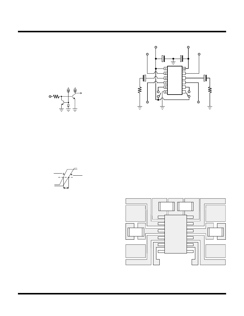
KEY INPUT CIRCUIT
1ch and 2ch is separate action by each control keys. Figure
11 is an equivalence circuit of key input. When terminal of
key is the open, is outputting high level (about 1.4 V), and
then Ach input signal is outputted. The channel at TK15326M
can be changed by high level.
SWITCHING TIME
This time is the signal change response time compared to
the control key input signal. Figure 12 illustrates the timimg
chart. T = 2
μ
s typically.
APPLICATION
Figure 13 illustrates an example of a typical application.
The standard application is to use direct coupling at GND
level at the inputs and outputs of the TK15326M. For
characteristics of distortion and dynamic range versus R
L
,
refer to the graphs in the Typical Performance Character-
istics. The TK15326M can be used at the capacitor
coupling too, but then the bias supply is necessary from the
GND level.
APPLICATION INFORMATION
Figure 11
Figure 12
Figure 13
Figure 14
CROSS TALK (ISOLATION AND SEPARATION)
Figure 14 is an example of a layout pattern. As the
TK15326M is a direct coupling type, the influence by
applications is not almost. But, if it is coupled at the
capacitor, by high impedance at input, capacitors
acccomplishes the antenna action each other. Then in
case its parts are bigger, and the space between capacitors
is too narrow, cross talk will increase. Therefore, when
designing the print circuit pattern, separate the input
capacitors as far as possible and use smaller parts. (e.g.,
surface mount type)
Key in
Bch (Ach)
SW out
50%
Ach (Bch)
t
1OUT
2AIN
VCC
GND
2OUT
1KEY
2KEY
2BIN
1AIN
1BIN
VEE
+
RL
10 μF
1Bin
11
10
9
8
7
2 Bin
1Key
2Key
+
RL
10 μF
+
33 μF
1Ain
2Ain
VCC
VEE
+
33 μF
Key in
to Logic
相關(guān)PDF資料 |
PDF描述 |
|---|---|
| TK15326M | Audio Analog Switch |
| TK15327 | Audio Analog Switch |
| TK15327M | Audio Analog Switch |
| TK15327MTL | Audio Analog Switch |
| TK15328 | Audio Analog Switch |
相關(guān)代理商/技術(shù)參數(shù) |
參數(shù)描述 |
|---|---|
| TK15326M | 制造商:TOKO 制造商全稱:TOKO, Inc 功能描述:Audio Analog Switch |
| TK15326MTL | 制造商:TOKO 制造商全稱:TOKO, Inc 功能描述:Audio Analog Switch |
| TK15326MTL/326 | 制造商:TOKO 制造商全稱:TOKO, Inc 功能描述:Audio Analog Switch |
| TK15327 | 制造商:TOKO 制造商全稱:TOKO, Inc 功能描述:Audio Analog Switch |
| TK15327M | 制造商:TOKO 制造商全稱:TOKO, Inc 功能描述:Audio Analog Switch |
發(fā)布緊急采購,3分鐘左右您將得到回復(fù)。