- 您現(xiàn)在的位置:買賣IC網(wǎng) > PDF目錄361482 > TK14551VTL (TOKO INC) FM IF DETECTOR/AMPLIFIER PDF資料下載
參數(shù)資料
| 型號: | TK14551VTL |
| 廠商: | TOKO INC |
| 元件分類: | 通信及網(wǎng)絡(luò) |
| 英文描述: | FM IF DETECTOR/AMPLIFIER |
| 中文描述: | SPECIALTY TELECOM CIRCUIT, PDSO24 |
| 封裝: | TSSOP-24 |
| 文件頁數(shù): | 26/32頁 |
| 文件大?。?/td> | 334K |
| 代理商: | TK14551VTL |
第1頁第2頁第3頁第4頁第5頁第6頁第7頁第8頁第9頁第10頁第11頁第12頁第13頁第14頁第15頁第16頁第17頁第18頁第19頁第20頁第21頁第22頁第23頁第24頁第25頁當(dāng)前第26頁第27頁第28頁第29頁第30頁第31頁第32頁
Page 26
January 2000 TOKO, Inc.
TK14551V
CIRCUIT DESCRIPTION
RSSI Comparator, Data Comparator:
The TK14551V contains a general purpose high speed data comparator and RSSI comparator for the base band
processing.
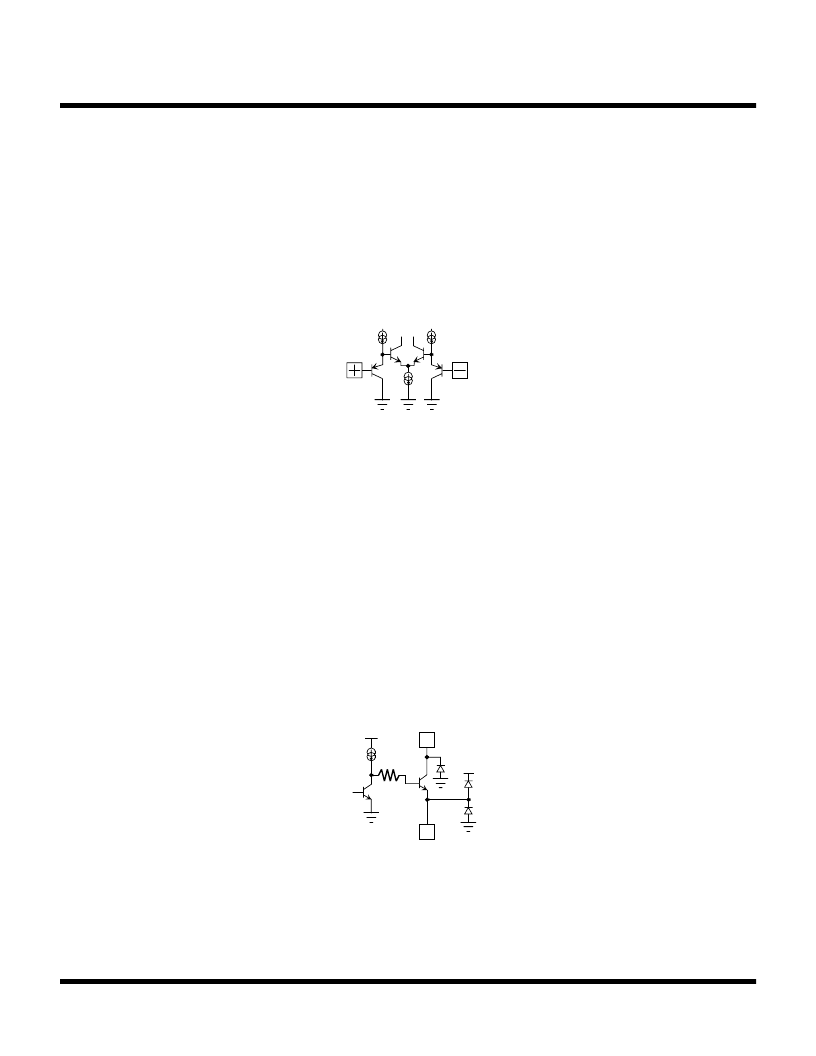
Because the input stage is composed of PNP transistors, it is possible to operate from a minimum voltage of 0.1 V to
the supply voltage - 1.0 V (see Figure 12).
Moreover, since the HFE of this PNP transistor is over 100, the bias current is below 0.01
μ
A (this is below the value of
the competitors products which typically use a lateral PNP transistor at the input stage).
Figure 13 shows the internal equivalent circuit of the comparator output stage. Because the comparator output is an open
collector, it is suitable for many interface levels. This open collector output is connected with an electrostatic discharge
protection diode at the GND side only; it is not connected with it at the power supply side in consideration of operating
the voltage over the supply voltage of this IC.
When the collector pull-up resistor value is low, high operating currents result. To prevent interference to the other
circuitry, the emitters of the output transistors are brought out independently at Pins 14 and 15.
Pins 14 and 15 are not connected with the substrate and other GNDs internal to the IC. Therefore, when operating these
comparators, these terminals must be connected to GND.
When these comparators are operating at high speed, the etch pattern of Pins 13, 14, 15, and 16 (comparator output
stages) should not be run close to the etch pattern of Pins 23 and 24 (IF inputs). The switching waveforms of the
comparator outputs may have an effect on the IF inputs and may add noise to the zero crossing of the demodulated
waveform, resulting in cross over distortion.
Because the negative input of the RSSI comparator is connected to the RSSI buffer amplifier output-1 internally, it is used
for carrier sensing.
The data comparator is used for the data shaper.
INPUT STAGE
FIGURE 12 - COMPARATOR INPUT STAGE
VCC
14,
15
13,
16
VCC
COMPARATOR
OUTPUT STAGE
FIGURE 13 - COMPARATOR OUTPUT STAGE
相關(guān)PDF資料 |
PDF描述 |
|---|---|
| TK14552V | Wide band AM / ASK IF IC for ETC |
| TK14584 | FM IF IC |
| TK14584M | FM IF IC |
| TK14584MTL | FM IF IC |
| TK14588 | FM IF IC |
相關(guān)代理商/技術(shù)參數(shù) |
參數(shù)描述 |
|---|---|
| TK14552V | 制造商:TOKO 制造商全稱:TOKO, Inc 功能描述:Wide band AM / ASK IF IC for ETC |
| TK14583V-G | 制造商:TOKO 制造商全稱:TOKO, Inc 功能描述:Wide band FM IF IC for remote keyless entry / tire pressure monitoring system |
| TK14583VTL-G | 制造商:TOKO 制造商全稱:TOKO, Inc 功能描述:Wide band FM IF IC for remote keyless entry / tire pressure monitoring system |
| TK14584 | 制造商:TOKO 制造商全稱:TOKO, Inc 功能描述:FM IF IC |
| TK14584M | 制造商:TOKO 制造商全稱:TOKO, Inc 功能描述:FM IF IC |
發(fā)布緊急采購,3分鐘左右您將得到回復(fù)。