- 您現(xiàn)在的位置:買(mǎi)賣(mài)IC網(wǎng) > PDF目錄98229 > THS8133BCPHPG4 (TEXAS INSTRUMENTS INC) PARALLEL, WORD INPUT LOADING, 0.005 us SETTLING TIME, 10-BIT DAC, PQFP48 PDF資料下載
參數(shù)資料
| 型號(hào): | THS8133BCPHPG4 |
| 廠商: | TEXAS INSTRUMENTS INC |
| 元件分類(lèi): | DAC |
| 英文描述: | PARALLEL, WORD INPUT LOADING, 0.005 us SETTLING TIME, 10-BIT DAC, PQFP48 |
| 封裝: | PLASTIC, HTQFP-48 |
| 文件頁(yè)數(shù): | 3/25頁(yè) |
| 文件大小: | 549K |
| 代理商: | THS8133BCPHPG4 |
第1頁(yè)第2頁(yè)當(dāng)前第3頁(yè)第4頁(yè)第5頁(yè)第6頁(yè)第7頁(yè)第8頁(yè)第9頁(yè)第10頁(yè)第11頁(yè)第12頁(yè)第13頁(yè)第14頁(yè)第15頁(yè)第16頁(yè)第17頁(yè)第18頁(yè)第19頁(yè)第20頁(yè)第21頁(yè)第22頁(yè)第23頁(yè)第24頁(yè)第25頁(yè)

THS8133, THS8133A, THS8133B
TRIPLE 10BIT, 80 MSPS VIDEO D/A CONVERTER
WITH TRILEVEL SYNC GENERATION
SLVS204C APRIL 1999 REVISED SEPTEMBER 2000
11
POST OFFICE BOX 655303
DALLAS, TEXAS 75265
POST OFFICE BOX 1443
HOUSTON, TEXAS 772511443
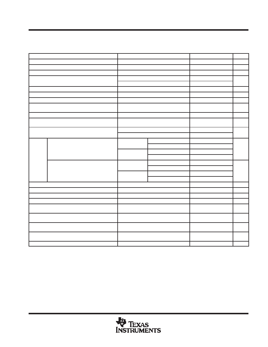
electrical characteristics over recommended operating conditions with fCLK = 80 MSPS and use
of internal reference voltage Vref, with R(FS) = R(FSnom) (unless otherwise noted) (continued)
analog (DAC) outputs
PARAMETER
TEST CONDITIONS
MIN
TYP
MAX
UNIT
DAC resolution
10
bits
INL
Integral nonlinearity
Static, best fit
±0.6
±1.2
LSB
DNL
Differential nonlinearity
Static
0.25/0.5
±1
LSB
PSRR
Power supply ripple rejection ratio of DAC
f = 100 kHz (see Note 4)
37
dB
PSRR
Power supply ripple rejection ratio of DAC
output (full scale)
f = 1 MHz (see Note 4)
43
dB
XTALK
Crosstalk between channels
f up to 30 MHz, (see Note 5)
55
dB
VO(ref)
Voltage reference output
1.30
1.35
1.40
V
ro(VREF)
VREF output resistance
7K
11K
15K
W
G(DAC)
DAC gain factor
See
Table 4
Imbalance between DACs, (KIMBAL)
See Note 6
±5%
Imbalance between positive and negative sync,
(KIMBAL(SYNC))
See Note 6
±2%
VO(DAC)
DAC output compliance voltage (sync+video)
RL = 37.5 , See Note 7
1
1.2
V
VO(DAC)
DAC output compliance voltage (sync+video)
RL = 75 , See Note 7
2
2.4
V
Internal reference
AGY
24
26.67
28
GBR sync-on-green and YPbPr sync-on-Y/sync-
Internal reference
ABPb and ARPr
17.3
18.67
19.7
mA
GBR sync-on-green and YPbPr sync-on-Y/sync-
on-all
External reference
AGY
24.9
26.67
27.2
mA
I(FS)
External reference
ABPb and ARPr
17.5
18.67
19.3
I(FS)
Internal reference
AGY
24
26.67
28
GBR sync-on-all
Internal reference
ABPb and ARPr
24
26.67
28
mA
GBR sync-on-all
External reference
AGY
24.9
26.67
27.2
mA
External reference
ABPb and ARPr
24.9
26.67
27.2
ro
DAC output resistance
See Note 10
57
92
k
CO
DAC output capacitance (pin capacitance)
8
pF
tr(DAC)
DAC output current rise time
10% to 90% of full scale
2
ns
tf(DAC)
DAC output current fall time
10% to 90% of full scale
2
ns
td(A)
Analog output delay
Measured from CLK=VIH(min) to 50% of full-scale
transition, See Note 8
9
ns
tS
Analog output settling time
Measured from 50% of full scale transition on
output to output settling, within 2%, See Note 9
5
9
ns
SNR
Signal -to-noise ratio
1 MHz, 1 dBFS digital sine input, measured from
0 MHz to 8.8 MHz
57.5
dB
SFDR
Spurious-free dynamic range
1MHz, 1 dBFS digital sine input, measured from
0 MHz to 8.8 MHz
64
dB
BW(1 dB)
Bandwidth
See Note 11
40
MHz
NOTES:
4. PSRR is measured with a 0.1
F capacitor between the COMP and AVDD terminal; with a 0.1 F capacitor connected between the VREF terminal and
AVSS. The ripple amplitude is within the range 100 mVp-p to 500 mVp-p with the DAC output set to full scale and a double-terminated 75
(=37.5 )
load. PSRR is defined as 20
× log(ripple voltage at DAC output/ripple voltage at AVDD input). Limits from characterization only.
5.
Crosstalk spec applies to each possible pair of the 3 DAC outputs. Limits from characterization only.
6.
The imbalance between DACs applies to all possible pairs of the three DACs. KIMBAL is assured over full temperature range. In parts labeled
THS8133CPHP, KIMBAL(SYNC) is assured at 25°C. In parts labeled THS8133ACPHP,KIMBAL(SYNC) and THS8133BCPHP,KIMBAL(SYNC) are assured
over the full temperature range.
7.
Nominal values at R(FS) = R(FSnom) : Maximum values at R(FS) = R(FSnom) ÷ 1.2. Maximum limits from characterization only.
8.
This value excludes the digital process delay, td(D). Limit from characterization only.
9.
Maximum limit from characterization only
10.
Limit from characterization only
11.
This bandwidth relates to the output amplitude variation in excess of the droop from the sinx/x sampled system. Since the output is a sample-and-hold
signal, a sin(
π × Fin ÷ Fclk) ÷ (π × Fin ÷ Fclk) roll-off is observed, which accounts e.g. at Fin = 40 MHz and Fclk = 80 MSPS for 3.92 dB signal drop (sync
droop). The total DAC output variation (device droop) consists of this and an additional amount (excess droop) caused by the output impedance of the
device, as shown in Table 5.
相關(guān)PDF資料 |
PDF描述 |
|---|---|
| THS8133CPHP | PARALLEL, WORD INPUT LOADING, 0.005 us SETTLING TIME, 10-BIT DAC, PQFP48 |
| THS8134BCPHP | PARALLEL, 8 BITS INPUT LOADING, 0.005 us SETTLING TIME, 8-BIT DAC, PQFP48 |
| THS8134CPHP | PARALLEL, 8 BITS INPUT LOADING, 0.005 us SETTLING TIME, 8-BIT DAC, PQFP48 |
| THS8134ACPHP | PARALLEL, 8 BITS INPUT LOADING, 0.005 us SETTLING TIME, 8-BIT DAC, PQFP48 |
| THS8135-240IPHP | PARALLEL, WORD INPUT LOADING, 10-BIT DAC, PQFP48 |
相關(guān)代理商/技術(shù)參數(shù) |
參數(shù)描述 |
|---|---|
| THS8133BEVM | 制造商:Texas Instruments 功能描述:THS8133B TRIPLE 10BIT 80MSPS VID DAC EVM - Bulk |
| THS8133CPHP | 制造商:TI 制造商全稱(chēng):Texas Instruments 功能描述:TRIPLE 10-BIT, 80 MSPS VIDEO D/A CONVERTER WITH TRI-LEVEL SYNC GENERATION |
| THS8133TQFP | 制造商:TI 制造商全稱(chēng):Texas Instruments 功能描述:TRIPLE 10-BIT, 80 MSPS VIDEO D/A CONVERTER WITH TRI-LEVEL SYNC GENERATION |
| THS8134 | 制造商:TI 制造商全稱(chēng):Texas Instruments 功能描述:TRIPLE 8-BIT, 80 MSPS VIDEO D/A CONVERTER WITH TRI-LEVEL SYNC GENERATION |
| THS8134A | 制造商:TI 制造商全稱(chēng):Texas Instruments 功能描述:TRIPLE 8-BIT, 80 MSPS VIDEO D/A CONVERTER WITH TRI-LEVEL SYNC GENERATION |
發(fā)布緊急采購(gòu),3分鐘左右您將得到回復(fù)。