- 您現(xiàn)在的位置:買賣IC網(wǎng) > PDF目錄98226 > THS4221DRG4 (TEXAS INSTRUMENTS INC) 1 CHANNEL, VIDEO PREAMPLIFIER, PDSO8 PDF資料下載
參數(shù)資料
| 型號: | THS4221DRG4 |
| 廠商: | TEXAS INSTRUMENTS INC |
| 元件分類: | 音頻/視頻放大 |
| 英文描述: | 1 CHANNEL, VIDEO PREAMPLIFIER, PDSO8 |
| 封裝: | GREEN, PLASTIC, MS-012AA, SOIC-8 |
| 文件頁數(shù): | 7/38頁 |
| 文件大?。?/td> | 1428K |
| 代理商: | THS4221DRG4 |
第1頁第2頁第3頁第4頁第5頁第6頁當前第7頁第8頁第9頁第10頁第11頁第12頁第13頁第14頁第15頁第16頁第17頁第18頁第19頁第20頁第21頁第22頁第23頁第24頁第25頁第26頁第27頁第28頁第29頁第30頁第31頁第32頁第33頁第34頁第35頁第36頁第37頁第38頁

THS4221, THS4225
THS4222, THS4226
SLOS399G AUGUST 2002 REVISED JANUARY 2004
www.ti.com
15
In the inverting configuration, some key design
considerations must be noted. One is that the gain resistor
(Rg) becomes part of the signal channel input impedance.
If the input impedance matching is desired (which is
beneficial whenever the signal is coupled through a cable,
twisted pair, long PC board trace, or other transmission
line conductors), Rg may be set equal to the required
termination value and Rf adjusted to give the desired gain.
However, care must be taken when dealing with low
inverting gains, as the resultant feedback resistor value
can present a significant load to the amplifier output. For
an inverting gain of 2, setting Rg to 49.9 for input
matching eliminates the need for RM but requires a 100-
feedback resistor. This has an advantage of the noise gain
becoming equal to 2 for a 50- source impedance—the
same as the noninverting circuit in Figure 29. However, the
amplifier output now sees the 100- feedback resistor in
parallel with the external load. To eliminate this excessive
loading, it is preferable to increase both Rg and Rf, values,
as shown in Figure 30, and then achieve the input
matching impedance with a third resistor (RM) to ground.
The total input impedance becomes the parallel
combination of Rg and RM.
The last major consideration to discuss in inverting
amplifier design is setting the bias current cancellation
resistor on the noninverting input. If the resistance is set
equal to the total dc resistance looking out of the inverting
terminal, the output dc error, due to the input bias currents,
is reduced to (input offset current) multiplied by Rf in
Figure 30, the dc source impedance looking out of the
inverting terminal is 1.3 k || (1.3 k + 25.6 ) = 649 .
To reduce the additional high-frequency noise introduced
by the resistor at the noninverting input, and power-supply
feedback, RT is bypassed with a capacitor to ground.
SINGLE SUPPLY OPERATION
The THS4222 is designed to operate from a single 3-V to
15-V power supply. When operating from a single power
supply, care must be taken to ensure the input signal and
amplifier are biased appropriately to allow for the
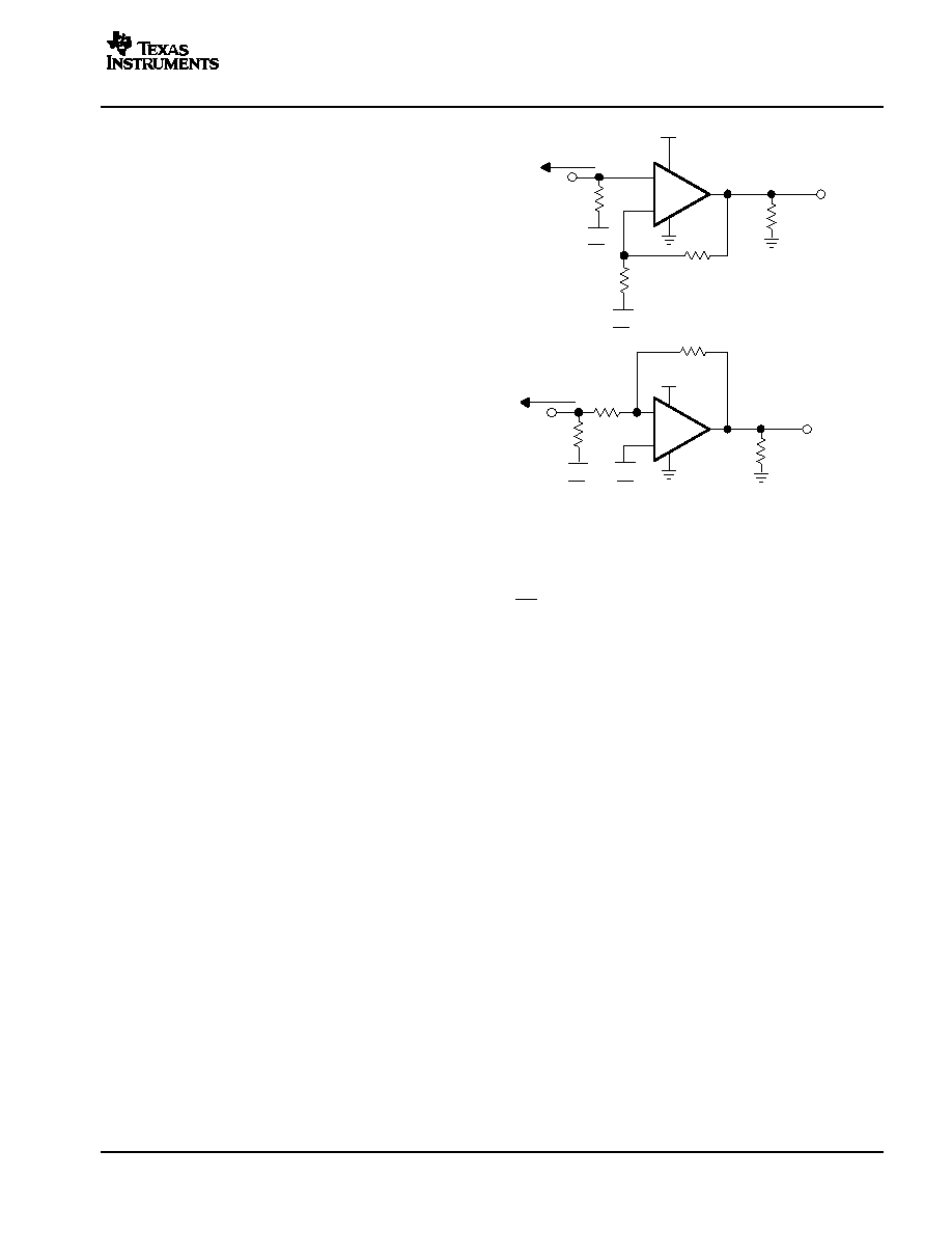
maximum output voltage swing. The circuits shown in
Figure 31 demonstrate methods to configure an amplifier
in a manner conducive for single supply operation.
_
+
THS4222
49.9
50 Source
VI
+VS
VO
Rf
1.3 k
Rg
1.3 k
+VS
2
+VS
2
_
+
THS4222
1.3 k
50 Source
VI
VS
VO
Rf
1.3 k
52.3
Rg
499
RT
499
RT
+VS
2
+VS
2
Figure 31. DC-Coupled Single Supply Operation
Saving Power With Power-Down Functionality
and Setting Threshold Levels With the Reference
Pin
The THS4225 and THS4226 feature a power-down pin
(PD) which lowers the quiescent current from 14 mA/ch
down to 700 A/ch, ideal for reducing system power.
The power-down pin of the amplifiers defaults to the
positive supply voltage in the absence of an applied
voltage, putting the amplifier in the power-on mode of
operation. To turn off the amplifier in an effort to conserve
power, the power-down pin can be driven towards the
negative rail. The threshold voltages for power-on and
power-down are relative to the supply rails and given in the
specification tables. Above the Enable Threshold Voltage,
the device is on. Below the Disable Threshold Voltage, the
device is off. Behavior in between these threshold voltages
is not specified.
Note that this power-down functionality is just that; the
amplifier consumes less power in power-down mode. The
power-down mode is not intended to provide a high-
impedance output. In other words, the power-down
functionality is not intended to allow use as a 3-state bus
driver. When in power-down mode, the impedance looking
back into the output of the amplifier is dominated by the
feedback and gain setting resistors, but the output
impedance of the device itself varies depending on the
voltage applied to the outputs.
The time delays associated with turning the device on and
off are specified as the time it takes for the amplifier to
reach 50% of the nominal quiescent current. The time
delays are on the order of microseconds because the
amplifier moves in and out of the linear mode of operation
in these transitions.
相關(guān)PDF資料 |
PDF描述 |
|---|---|
| THS4225DRG4 | 1 CHANNEL, VIDEO PREAMPLIFIER, PDSO8 |
| THS4271DGKG4 | 1 CHANNEL, VIDEO PREAMPLIFIER, PDSO8 |
| THS4271DGNG4 | 1 CHANNEL, VIDEO PREAMPLIFIER, PDSO8 |
| THS4271DRBRG4 | 1 CHANNEL, VIDEO PREAMPLIFIER, PDSO8 |
| THS4271DRBTG4 | 1 CHANNEL, VIDEO PREAMPLIFIER, PDSO8 |
相關(guān)代理商/技術(shù)參數(shù) |
參數(shù)描述 |
|---|---|
| THS4221EVM | 功能描述:放大器 IC 開發(fā)工具 THS4221 Eval Mod RoHS:否 制造商:International Rectifier 產(chǎn)品:Demonstration Boards 類型:Power Amplifiers 工具用于評估:IR4302 工作電源電壓:13 V to 23 V |
| THS4222 | 制造商:TI 制造商全稱:Texas Instruments 功能描述:LOW-DISTORTION, HIGH-SPEED, RAIL-TO-RAIL OUTPUT OPERATIONAL AMPLIFIERS |
| THS4222D | 功能描述:高速運算放大器 Low-Distortion High- Speed R-to-R Output RoHS:否 制造商:Texas Instruments 通道數(shù)量:1 電壓增益 dB:116 dB 輸入補償電壓:0.5 mV 轉(zhuǎn)換速度:55 V/us 工作電源電壓:36 V 電源電流:7.5 mA 最大工作溫度:+ 85 C 安裝風格:SMD/SMT 封裝 / 箱體:SOIC-8 封裝:Tube |
| THS4222DG4 | 功能描述:高速運算放大器 Low-Distortion High- Speed R-to-R Output RoHS:否 制造商:Texas Instruments 通道數(shù)量:1 電壓增益 dB:116 dB 輸入補償電壓:0.5 mV 轉(zhuǎn)換速度:55 V/us 工作電源電壓:36 V 電源電流:7.5 mA 最大工作溫度:+ 85 C 安裝風格:SMD/SMT 封裝 / 箱體:SOIC-8 封裝:Tube |
| THS4222DGK | 功能描述:高速運算放大器 Low-Distortion High- Speed R-to-R Output RoHS:否 制造商:Texas Instruments 通道數(shù)量:1 電壓增益 dB:116 dB 輸入補償電壓:0.5 mV 轉(zhuǎn)換速度:55 V/us 工作電源電壓:36 V 電源電流:7.5 mA 最大工作溫度:+ 85 C 安裝風格:SMD/SMT 封裝 / 箱體:SOIC-8 封裝:Tube |
發(fā)布緊急采購,3分鐘左右您將得到回復(fù)。