- 您現(xiàn)在的位置:買賣IC網(wǎng) > PDF目錄383996 > THS4082EVM (Texas Instruments, Inc.) 175-MHz LOW-POWER HIGH-SPEED AMPLIFIERS PDF資料下載
參數(shù)資料
| 型號: | THS4082EVM |
| 廠商: | Texas Instruments, Inc. |
| 英文描述: | 175-MHz LOW-POWER HIGH-SPEED AMPLIFIERS |
| 中文描述: | 175 - MHz的低功耗高速放大器 |
| 文件頁數(shù): | 19/24頁 |
| 文件大小: | 384K |
| 代理商: | THS4082EVM |
THS4081, THS4082
175-MHz LOW-POWER HIGH-SPEED AMPLIFIERS
SLOS274C – DECEMBER 1999 – REVISED MAY 2000
19
POST OFFICE BOX 655303
DALLAS, TEXAS 75265
APPLICATION INFORMATION
general PowerPAD
design considerations (continued)
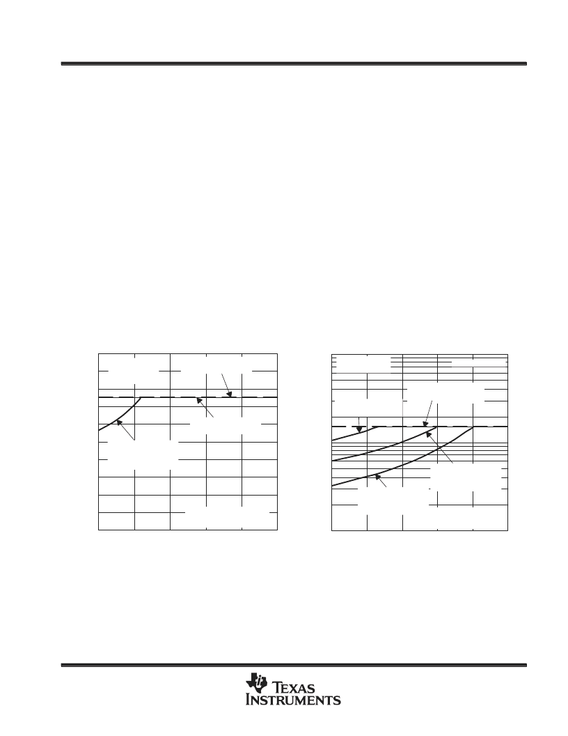
The next consideration is the package constraints. The two sources of heat within an amplifier are quiescent
power and output power. The designer should never forget about the quiescent heat generated within the
device, especially multiamplifier devices. Because these devices have linear output stages (Class A-B), most
of the heat dissipation is at low output voltages with high output currents. Figure 47 to Figure 50 show this effect,
along with the quiescent heat, with an ambient air temperature of 50
°
C. Obviously, as the ambient temperature
increases, the limit lines shown will drop accordingly. The area under each respective limit line is considered
the safe operating area. Any condition above this line will exceed the amplifier’s limits and failure may result.
When using V
CC
=
±
5 V, there is generally not a heat problem, even with SOIC packages. But, when using V
CC
=
±
15 V, the SOIC package is severely limited in the amount of heat it can dissipate. The other key factor when
looking at these graphs is how the devices are mounted on the PCB. The PowerPAD
devices are extremely
useful for heat dissipation. But, the device should always be soldered to a copper plane to fully use the heat
dissipation properties of the PowerPAD
. The SOIC package, on the other hand, is highly dependent on how
it is mounted on the PCB. As more trace and copper area is placed around the device,
θ
JA
decreases and the
heat dissipation capability increases. The currents and voltages shown in these graphs are for the total package.
For the dual amplifier package (THS4082), the sum of the RMS output currents and voltages should be used
to choose the proper package. The graphs shown assume that both amplifier’s outputs are identical.
Figure 47
Package With
θ
JA < = 127
°
C/W
SO-8 Package
θ
JA = 167
°
C/W
Low-K Test PCB
VCC =
±
5 V
TJ = 150
°
C
TA = 50
°
C
100
80
40
0
0
1
| VO | – RMS Output Voltage – V
2
3
–
IO
|
140
180
200
4
5
160
120
60
20
|
Maximum Output
Current Limit Line
THS4081
MAXIMUM RMS OUTPUT CURRENT
vs
RMS OUTPUT VOLTAGE DUE TO THERMAL LIMITS
Safe Operating
Area
Figure 48
100
10
0
3
| VO | – RMS Output Voltage – V
6
9
1000
12
15
Maximum Output
Current Limit Line
SO-8 Package
θ
JA = 167
°
C/W
Low-K Test PCB
SO-8 Package
θ
JA = 98
°
C/W
High-K Test PCB
TJ = 150
°
C
TA = 50
°
C
–
IO
|
|
VCC =
±
15 V
DGN Package
θ
JA = 58.4
°
C/W
THS4081
MAXIMUM RMS OUTPUT CURRENT
vs
RMS OUTPUT VOLTAGE DUE TO THERMAL LIMITS
Safe Operating
Area
相關(guān)PDF資料 |
PDF描述 |
|---|---|
| THS4081D | 175-MHz LOW-POWER HIGH-SPEED AMPLIFIERS |
| THS4081DGN | 175-MHz LOW-POWER HIGH-SPEED AMPLIFIERS |
| THS4081EVM | 175-MHz LOW-POWER HIGH-SPEED AMPLIFIERS |
| THS4130EVM | HIGH SPEED LOW NOISE, FULLY DIFFERENTIAL I/O AMPLIFIERS |
| THS4211DGKR | LOW-DISTORTION HIGH-SPEED VOLTAGE FEEDBACK AMPLIFIER |
相關(guān)代理商/技術(shù)參數(shù) |
參數(shù)描述 |
|---|---|
| THS4082ID | 功能描述:高速運(yùn)算放大器 Dual 175MHz RoHS:否 制造商:Texas Instruments 通道數(shù)量:1 電壓增益 dB:116 dB 輸入補(bǔ)償電壓:0.5 mV 轉(zhuǎn)換速度:55 V/us 工作電源電壓:36 V 電源電流:7.5 mA 最大工作溫度:+ 85 C 安裝風(fēng)格:SMD/SMT 封裝 / 箱體:SOIC-8 封裝:Tube |
| THS4082IDG4 | 功能描述:高速運(yùn)算放大器 175-MHz Low-Power Vltg-Feedback Dual RoHS:否 制造商:Texas Instruments 通道數(shù)量:1 電壓增益 dB:116 dB 輸入補(bǔ)償電壓:0.5 mV 轉(zhuǎn)換速度:55 V/us 工作電源電壓:36 V 電源電流:7.5 mA 最大工作溫度:+ 85 C 安裝風(fēng)格:SMD/SMT 封裝 / 箱體:SOIC-8 封裝:Tube |
| THS4082IDGN | 功能描述:高速運(yùn)算放大器 175-MHz Low-Power Vltg-Feedback Dual RoHS:否 制造商:Texas Instruments 通道數(shù)量:1 電壓增益 dB:116 dB 輸入補(bǔ)償電壓:0.5 mV 轉(zhuǎn)換速度:55 V/us 工作電源電壓:36 V 電源電流:7.5 mA 最大工作溫度:+ 85 C 安裝風(fēng)格:SMD/SMT 封裝 / 箱體:SOIC-8 封裝:Tube |
| THS4082IDGNG4 | 功能描述:高速運(yùn)算放大器 175-MHz Low-Power Vltg-Feedback Dual RoHS:否 制造商:Texas Instruments 通道數(shù)量:1 電壓增益 dB:116 dB 輸入補(bǔ)償電壓:0.5 mV 轉(zhuǎn)換速度:55 V/us 工作電源電壓:36 V 電源電流:7.5 mA 最大工作溫度:+ 85 C 安裝風(fēng)格:SMD/SMT 封裝 / 箱體:SOIC-8 封裝:Tube |
| THS4082IDGNR | 功能描述:高速運(yùn)算放大器 175-MHz Low-Power Vltg-Feedback Dual RoHS:否 制造商:Texas Instruments 通道數(shù)量:1 電壓增益 dB:116 dB 輸入補(bǔ)償電壓:0.5 mV 轉(zhuǎn)換速度:55 V/us 工作電源電壓:36 V 電源電流:7.5 mA 最大工作溫度:+ 85 C 安裝風(fēng)格:SMD/SMT 封裝 / 箱體:SOIC-8 封裝:Tube |
發(fā)布緊急采購,3分鐘左右您將得到回復(fù)。