- 您現(xiàn)在的位置:買賣IC網(wǎng) > PDF目錄98219 > THS1209CDA (TEXAS INSTRUMENTS INC) 2-CH 12-BIT PROPRIETARY METHOD ADC, PARALLEL ACCESS, PDSO32 PDF資料下載
參數(shù)資料
| 型號(hào): | THS1209CDA |
| 廠商: | TEXAS INSTRUMENTS INC |
| 元件分類: | ADC |
| 英文描述: | 2-CH 12-BIT PROPRIETARY METHOD ADC, PARALLEL ACCESS, PDSO32 |
| 封裝: | GREEN, PLASTIC, TSSOP-32 |
| 文件頁數(shù): | 13/33頁 |
| 文件大小: | 312K |
| 代理商: | THS1209CDA |
第1頁第2頁第3頁第4頁第5頁第6頁第7頁第8頁第9頁第10頁第11頁第12頁當(dāng)前第13頁第14頁第15頁第16頁第17頁第18頁第19頁第20頁第21頁第22頁第23頁第24頁第25頁第26頁第27頁第28頁第29頁第30頁第31頁第32頁第33頁

THS1209
SLAS288B – JULY 2000 – REVISED DECEMBER 2002
www.ti.com
20
ADC CONTROL REGISTERS
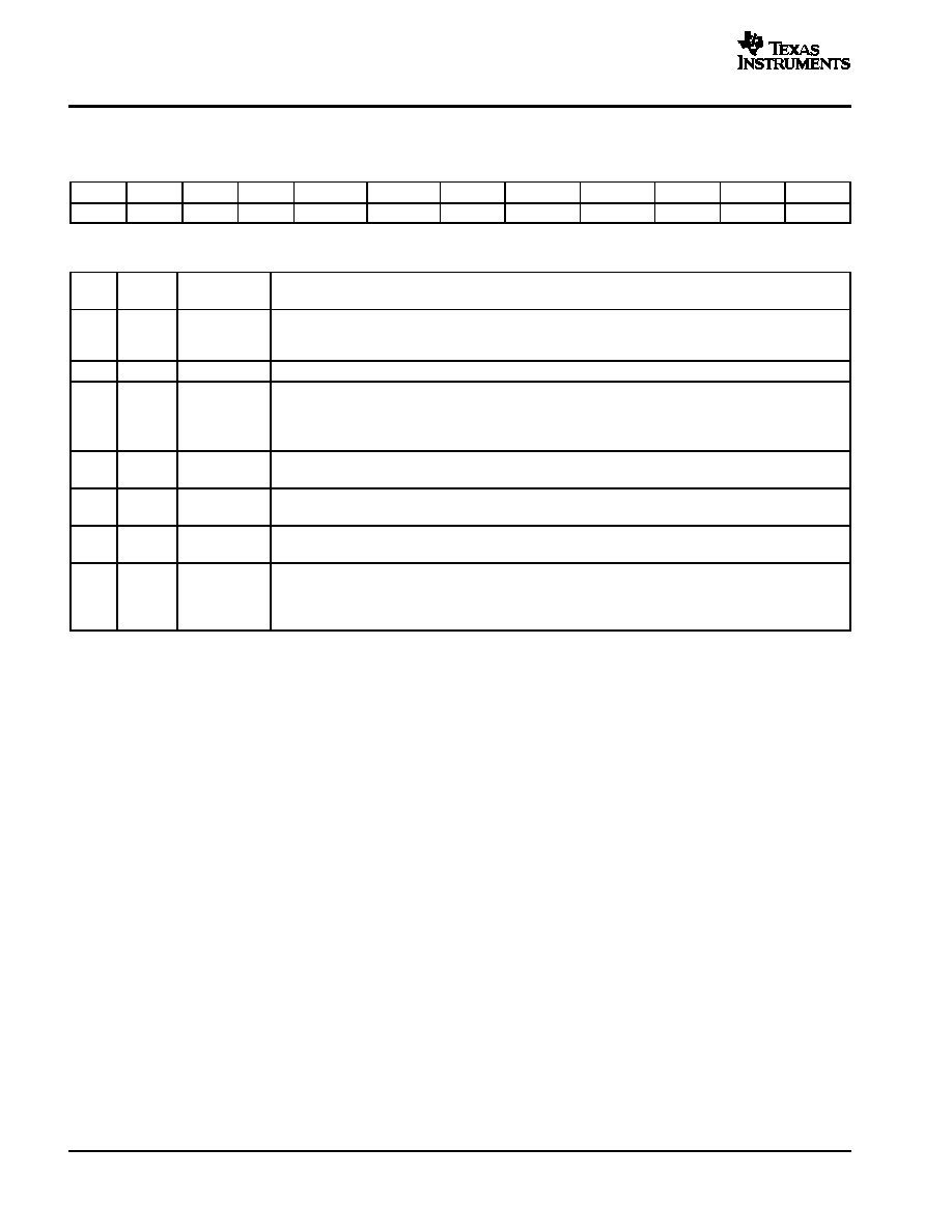
Control Register 0 (see Table 8)
BIT 11
BIT 10
BIT 9
BIT 8
BIT 7
BIT 6
BIT 5
BIT 4
BIT 3
BIT 2
BIT 1
BIT 0
0
TEST1
TEST0
SCAN
DIFF1
DIFF0
CHSEL1
CHSEL0
PD
RES
VREF
Table 8. Control Register 0 Bit Functions
BITS
RESET
VALUE
NAME
FUNCTION
0
VREF
Vref select:
Bit 0 = 0
→ The internal reference is selected.
Bit 0 = 1
→ The external reference voltage is selected.
1
0
RES
Reserved
2
0
PD
Power down.
Bit 2 = 0
→ The ADC is active.
Bit 2 = 1
→ Power down
The reading and writing to and from the digital outputs is possible during power down.
3, 4
0,0
CHSEL0,
CHSEL1
Channel select
Bit 3 and bit 4 select the analog input channel of the ADC. Refer to Table 9.
5,6
1,0
DIFF0, DIFF1
Number of differential channels
Bit 5 and bit 6 contain information about the number of selected differential channels. Refer to Table 9.
7
0
SCAN
Autoscan enable
Bit 7 enables or disables the autoscan function of the ADC. Refer to Table 9.
8,9
0,0
TEST0,
TEST1
Test input enable
Bit 8 and bit 9 control the test function of the ADC. Three different test voltages can be measured. This
feedback allows the check of all hardware connections and the ADC operation.
Refer to Table 10 for selection of the three different test voltages.
發(fā)布緊急采購,3分鐘左右您將得到回復(fù)。