- 您現(xiàn)在的位置:買賣IC網(wǎng) > PDF目錄98217 > THS10082IDA (TEXAS INSTRUMENTS INC) 2-CH 10-BIT PROPRIETARY METHOD ADC, PARALLEL ACCESS, PDSO32 PDF資料下載
參數(shù)資料
| 型號(hào): | THS10082IDA |
| 廠商: | TEXAS INSTRUMENTS INC |
| 元件分類: | ADC |
| 英文描述: | 2-CH 10-BIT PROPRIETARY METHOD ADC, PARALLEL ACCESS, PDSO32 |
| 封裝: | GREEN, PLASTIC, TSSOP-32 |
| 文件頁(yè)數(shù): | 8/37頁(yè) |
| 文件大小: | 350K |
| 代理商: | THS10082IDA |
第1頁(yè)第2頁(yè)第3頁(yè)第4頁(yè)第5頁(yè)第6頁(yè)第7頁(yè)當(dāng)前第8頁(yè)第9頁(yè)第10頁(yè)第11頁(yè)第12頁(yè)第13頁(yè)第14頁(yè)第15頁(yè)第16頁(yè)第17頁(yè)第18頁(yè)第19頁(yè)第20頁(yè)第21頁(yè)第22頁(yè)第23頁(yè)第24頁(yè)第25頁(yè)第26頁(yè)第27頁(yè)第28頁(yè)第29頁(yè)第30頁(yè)第31頁(yè)第32頁(yè)第33頁(yè)第34頁(yè)第35頁(yè)第36頁(yè)第37頁(yè)

THS10082
SLAS254B MAY 2002 REVISED NOVEMBER 2002
www.ti.com
16
SINGLE CONVERSION MODE
In single conversion mode, a single conversion of the selected analog input channels is performed. The single conversion
mode is selected by setting bit 1 of control register 0 to 1.
A single conversion is initiated by pulsing the CONVST input. On the falling edge of CONVST, the sample and hold stages
of the selected analog inputs are placed into hold simultaneously, and the conversion sequence for the selected channels
is started.
The conversion clock in single conversion mode is generated internally using a clock oscillator circuit. The signal DATA_AV
(data available) becomes active when the trigger level is reached and indicates that the converted sample(s) is (are) written
into the FIFO and can be read out. The trigger level in the single conversion mode can be selected according to Table 13.
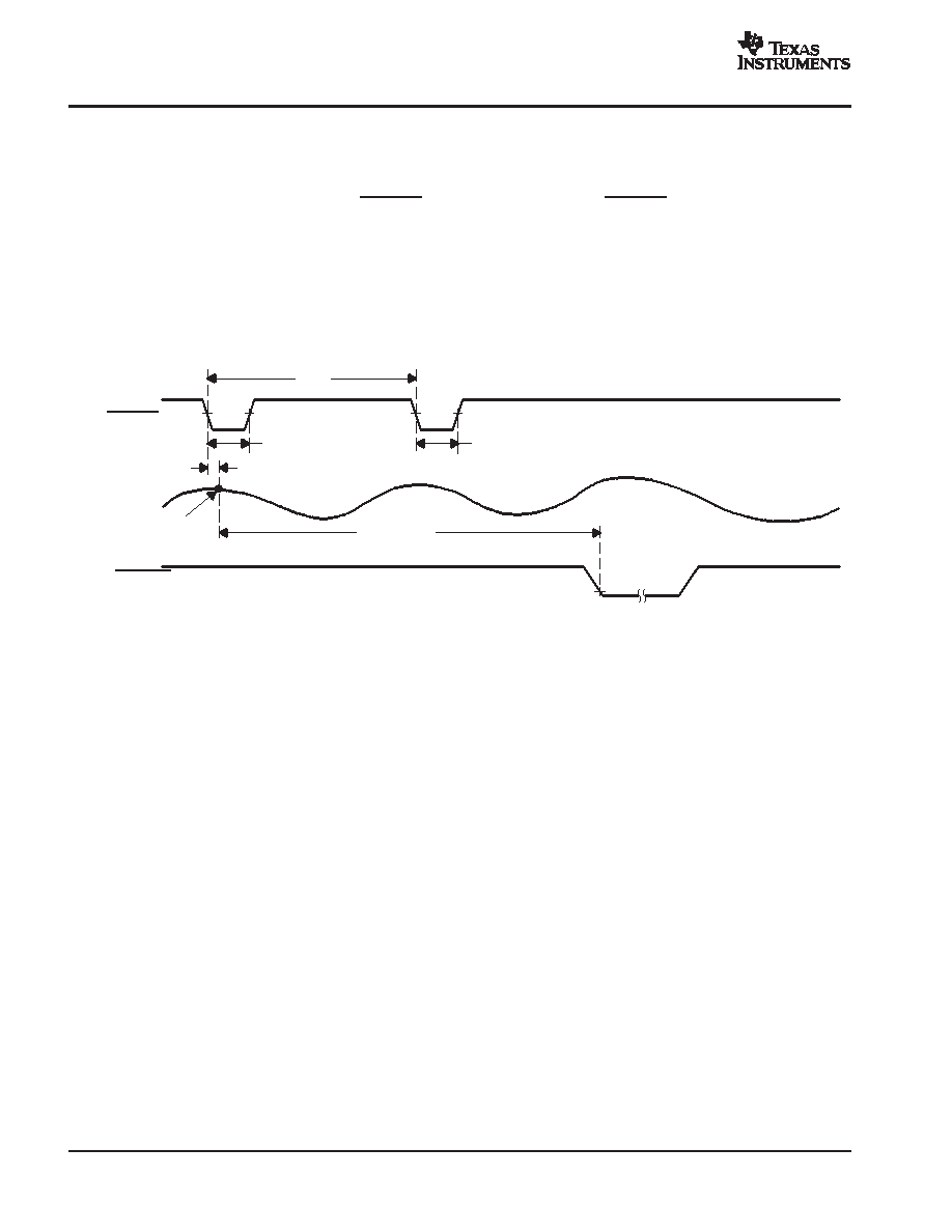
Figure 26 shows the timing of the single conversion mode. In this mode, up to two analog input channels can be selected
to be sampled simultaneously (see Table 2).
CONVST
AIN
Sample N
t1
td(A)
t2
tDATA_AV
DATA_AV,
Trigger Level = 1
Figure 26. Timing of Single Conversion Mode
The time (t2) between consecutive starts of single conversions is dependent on the number of selected analog input
channels. The time tDATA_AV, until DATA_AV becomes active is given by: tDATA_AV = tpipe + n × tc. This equation is valid for
a trigger level which is equivalent to the number of selected analog input channels. For all other trigger level conditions refer
to the timing specifications of single conversion mode.
CONTINUOUS CONVERSION MODE
The internal clock oscillator used in the single-conversion mode is switched off in continuous conversion mode. In
continuous conversion mode, (bit 1 of control register 0 set to 0) the ADC operates with a free running external clock signal
CONV_CLK. With every rising edge of the CONV_CLK signal a new converted value is written into the FIFO.
Figure 27 shows the timing of continuous conversion mode when one analog input channel is selected. The maximum
throughput rate is 8 MSPS in this mode. The timing of the DATA_AV signal is shown here in the case of a trigger level set
to 1 or 4.
相關(guān)PDF資料 |
PDF描述 |
|---|---|
| THS10082IDAR | 2-CH 10-BIT PROPRIETARY METHOD ADC, PARALLEL ACCESS, PDSO32 |
| THS10082IDAG4 | 2-CH 10-BIT PROPRIETARY METHOD ADC, PARALLEL ACCESS, PDSO32 |
| THS1009CDAR | 2-CH 10-BIT PROPRIETARY METHOD ADC, PARALLEL ACCESS, PDSO32 |
| THS1009CDA | 2-CH 10-BIT PROPRIETARY METHOD ADC, PARALLEL ACCESS, PDSO32 |
| THS1009IDA | 2-CH 10-BIT PROPRIETARY METHOD ADC, PARALLEL ACCESS, PDSO32 |
相關(guān)代理商/技術(shù)參數(shù) |
參數(shù)描述 |
|---|---|
| THS10082IDAG4 | 功能描述:模數(shù)轉(zhuǎn)換器 - ADC 10 Bit 8 MSPS Lo-Pwr RoHS:否 制造商:Texas Instruments 通道數(shù)量:2 結(jié)構(gòu):Sigma-Delta 轉(zhuǎn)換速率:125 SPs to 8 KSPs 分辨率:24 bit 輸入類型:Differential 信噪比:107 dB 接口類型:SPI 工作電源電壓:1.7 V to 3.6 V, 2.7 V to 5.25 V 最大工作溫度:+ 85 C 安裝風(fēng)格:SMD/SMT 封裝 / 箱體:VQFN-32 |
| THS1009 | 制造商:TI 制造商全稱:Texas Instruments 功能描述:10-BIT, 2 ANALOG INPUT, 8 MSPS, SIMULTANEOUS SAMPLING ANALOG-TO-DIGITAL CONVERTER |
| THS1009CDA | 制造商:TI 制造商全稱:Texas Instruments 功能描述:10-BIT, 2 ANALOG INPUT, 8 MSPS, SIMULTANEOUS SAMPLING ANALOG-TO-DIGITAL CONVERTER |
| THS1009CDAG4 | 制造商:TI 制造商全稱:Texas Instruments 功能描述:10-BIT, 2 ANALOG INPUT, 8 MSPS, SIMULTANEOUS SAMPLING ANALOG-TO-DIGITAL CONVERTER |
| THS1009CDAR | 制造商:TI 制造商全稱:Texas Instruments 功能描述:10-BIT, 2 ANALOG INPUT, 8 MSPS, SIMULTANEOUS SAMPLING ANALOG-TO-DIGITAL CONVERTER |
發(fā)布緊急采購(gòu),3分鐘左右您將得到回復(fù)。