- 您現(xiàn)在的位置:買(mǎi)賣(mài)IC網(wǎng) > PDF目錄98214 > TFDS5500-TR3 (VISHAY TELEFUNKEN) TRANSMITTER/RECEIVER IC, DMA8 PDF資料下載
參數(shù)資料
| 型號(hào): | TFDS5500-TR3 |
| 廠商: | VISHAY TELEFUNKEN |
| 元件分類(lèi): | 搖控器 |
| 英文描述: | TRANSMITTER/RECEIVER IC, DMA8 |
| 封裝: | 13 X 5.30 MM, 5.95 MM HEIGHT, STAGGERED, SMT-8 |
| 文件頁(yè)數(shù): | 10/13頁(yè) |
| 文件大?。?/td> | 257K |
| 代理商: | TFDS5500-TR3 |
第1頁(yè)第2頁(yè)第3頁(yè)第4頁(yè)第5頁(yè)第6頁(yè)第7頁(yè)第8頁(yè)第9頁(yè)當(dāng)前第10頁(yè)第11頁(yè)第12頁(yè)第13頁(yè)

TFDU5100/TFDS5500/TFDT5500
Vishay Telefunken
Not for new design
Rev. 1, 01-Apr-99
6
www.vishay.de
FaxBack +1-408-970-5600
Document Number 82516
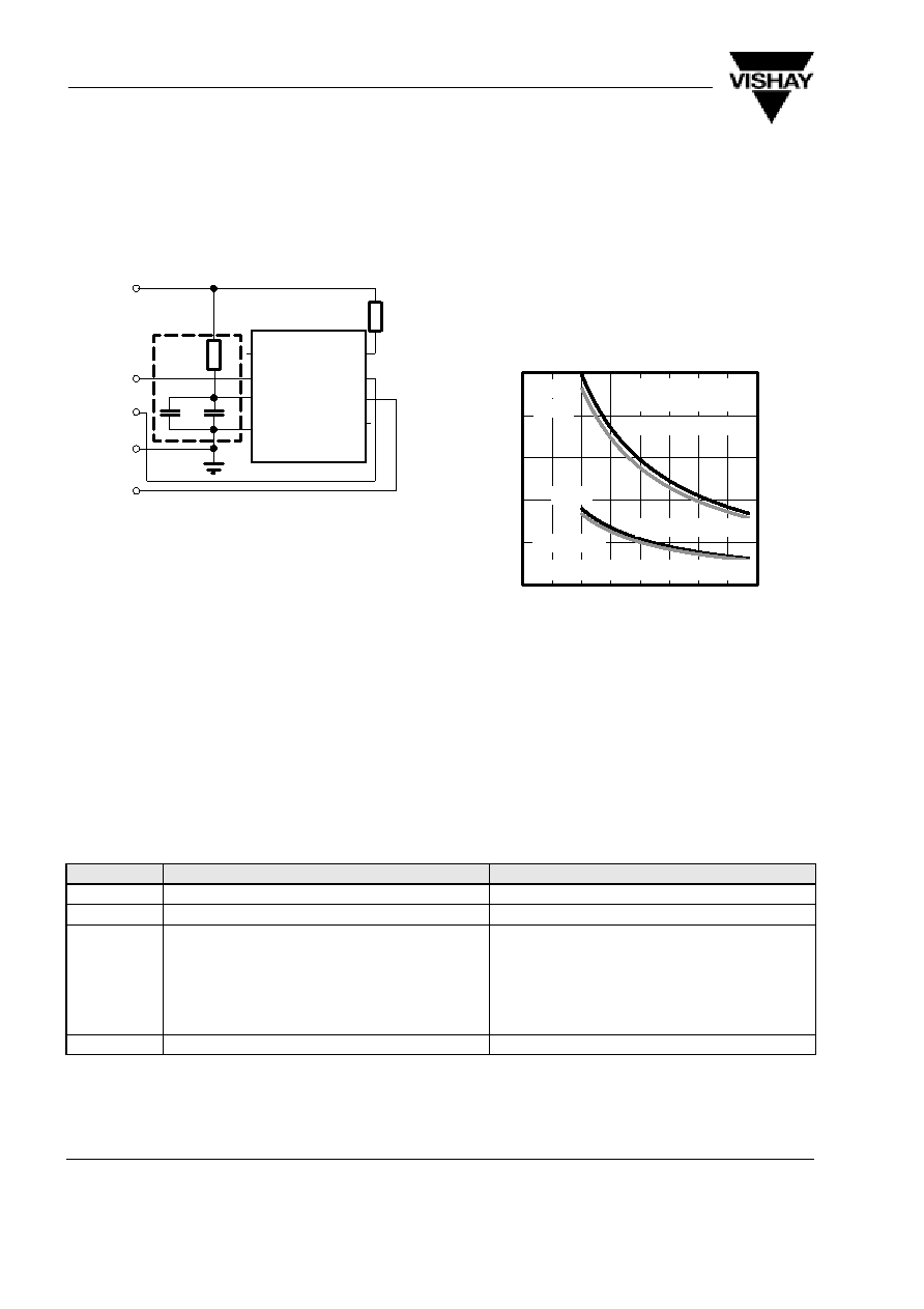
Recommended Circuit Diagram
The only required component for designing an
IrDA 1.2 compatible design using Vishay Telefunken
FIR transceivers is a current limiting resistor, R1, to the
IRED. However, depending on the entire system
design and board layout, additional components may
be required (see figure 3).
Mode
Txd
SD/Mode
GND
VCC
IRED
Cathode
Rxd
IRED
Anode
TFDx5x00
R1
C1
C2
R2
VCC
Rxd
Txd
GND
SD/Mode
Note: Outlined components are optional depending
on the quality of the power supply.
14911
Figure 3. Recommended Application Circuit
Vishay Telefunken transceivers integrate a sensitive
receiver and a built–in power driver. The combination
of both needs a careful circuit board layout. The use of
thin, long resistive and inductive wiring should be
avoided. The inputs (Txd, SD/Mode) and the output
Rxd should be directly (DC) coupled to the I/O circuit.
R1 is used for controlling the current through the IR
emitter. For increasing the output power of the IRED,
the value of the resistor should be reduced. Similarly,
to reduce the output power of the IRED, the value of
the resistor should be increased. For typical values of
R1 see figure 4. For IrDA compliant operation, a
current control resistor of 7.2
is recommended. The
upper drive current limitation is dependent on the duty
cycle and is given by the absolute maximum ratings on
the data sheet.
R2, C1 and C2 are optional and dependent on the
quality of the supply voltage VCC and injected noise.
An unstable power supply with dropping voltage during
transmission may reduce sensitivity (and transmission
range) of the transceiver.
0
100
200
300
400
500
02468
10
12
14
16
Current Control Resistor (
W )
14379
Intensity
(mW/sr)
min. intensity in emission cone
"15
°
max.Rdson, max.VF
max. intensity in
emission cone
"15°
Vcc=4.75V
min. Rdson, min. VF
5.0V
5.25V
Figure 4. Intensity Ie vs. Current Control Resistor R1
The placement of these parts is critical. It is strongly
recommended to position C2 as near as possible to the
transceiver
power
supply
pins.
An
electrolytic
capacitor should be used for C1 while a ceramic
capacitor is used for C2. Also, when connecting the
described circuit to the power supply, low impedance
wiring should be used.
Table 1. Recommended Application Circuit Components
Component
Recommended Value
Vishay Part Number
C1
4.7
mF, 16 V
293D 475X9 016B 2T
C2
0.1
F, Ceramic
VJ 1206 Y 104 J XXMT
R1
5 V supply voltage: 7.2
, 0.25 W
(recommend using
two 3.6
W, 0.125 W resistors in series)
3.3 V supply voltage: 3.6
, 0.25 W
(recommend using
two 1.8
W, 0.125 W resistors in series)
CRCW–1206–3R60–F–RT1
CRCW–1206–1R80–F–RT1
R2
47
, 0.125 W
CRCW–1206–47R0–F–RT1
相關(guān)PDF資料 |
PDF描述 |
|---|---|
| TFDT5500-TR3 | TRANSMITTER/RECEIVER IC, SMA8 |
| TFDU5100-TR3 | TRANSMITTER/RECEIVER IC, SMA8 |
| TFDU5100-TT3 | TRANSMITTER/RECEIVER IC, SMA8 |
| TFDS5500-TR3 | INFRARED, TRANSMITTER/RECEIVER IC, SMA8 |
| TFDT5500-TR3 | INFRARED, TRANSMITTER/RECEIVER IC, SMA8 |
相關(guān)代理商/技術(shù)參數(shù) |
參數(shù)描述 |
|---|---|
| TFDS6401 | 制造商:VISHAY 制造商全稱:Vishay Siliconix 功能描述:Fast Infrared Transceiver Module Family (FIR, 4 Mbit/s) for 2.6 V to 5.5 V Operation |
| TFDS6401-TR3 | 制造商:VISHAY 制造商全稱:Vishay Siliconix 功能描述:Fast Infrared Transceiver Module Family (FIR, 4 Mbit/s) for 2.6 V to 5.5 V Operation |
| TFDS6402 | 制造商:VISHAY 制造商全稱:Vishay Siliconix 功能描述:Fast Infrared Transceiver Module Family (FIR, 4 Mbit/s) for 2.6 V to 5.5 V Operation |
| TFDS6402-TR3 | 制造商:VISHAY 制造商全稱:Vishay Siliconix 功能描述:Fast Infrared Transceiver Module Family (FIR, 4 Mbit/s) for 2.6 V to 5.5 V Operation |
| TFDS6500E | 制造商:VISHAY 制造商全稱:Vishay Siliconix 功能描述:2.7-5.5V Fast Infrared Transceiver Module Family |
發(fā)布緊急采購(gòu),3分鐘左右您將得到回復(fù)。