- 您現(xiàn)在的位置:買賣IC網(wǎng) > PDF目錄383993 > TE28F800B3TA90 (INTEL CORP) 3 Volt Advanced Boot Block Flash Memory PDF資料下載
參數(shù)資料
| 型號(hào): | TE28F800B3TA90 |
| 廠商: | INTEL CORP |
| 元件分類: | DRAM |
| 英文描述: | 3 Volt Advanced Boot Block Flash Memory |
| 中文描述: | 512K X 16 FLASH 2.7V PROM, 90 ns, PDSO48 |
| 封裝: | 12 X 20 MM, TSOP-48 |
| 文件頁數(shù): | 14/49頁 |
| 文件大小: | 427K |
| 代理商: | TE28F800B3TA90 |
第1頁第2頁第3頁第4頁第5頁第6頁第7頁第8頁第9頁第10頁第11頁第12頁第13頁當(dāng)前第14頁第15頁第16頁第17頁第18頁第19頁第20頁第21頁第22頁第23頁第24頁第25頁第26頁第27頁第28頁第29頁第30頁第31頁第32頁第33頁第34頁第35頁第36頁第37頁第38頁第39頁第40頁第41頁第42頁第43頁第44頁第45頁第46頁第47頁第48頁第49頁
SMART 3 ADVANCED BOOT BLOCK
–WORD-WIDE
E
14
PRELIMINARY
3.0
PRINCIPLES OF OPERATION
Flash memory combines EEPROM functionality
with in-circuit electrical program and erase
capability. The Smart 3 Advanced Boot Block flash
memory family utilizes a Command User Interface
(CUI) and automated algorithms to simplify program
and erase operations. The CUI allows for 100%
CMOS-level control inputs, fixed power supplies
during erasure and programming, and maximum
EEPROM compatibility.
When V
PP
< V
PPLK
, the device will only execute the
following commands successfully: Read Array,
Read Status Register, Clear Status Register and
Read Intelligent Identifier. The device provides
standard EEPROM read, standby and output
disable operations. Manufacturer identification and
device identification data can be accessed through
the CUI. In addition, 2.7V or 12V on V
PP
allows
program and erase of the device. All functions
associated with altering memory contents, namely
program and erase, are accessible via the CUI.
The internal Write State Machine (WSM) completely
automates program and erase operations while the
CUI signals the start of an operation and the status
register reports status. The CUI handles the WE#
interface to the data and address latches, as well
as system status requests during WSM operation.
3.1
Bus Operation
Smart 3 Advanced Boot Block flash memory
devices read, program and erase in-system via the
local CPU or microcontroller. All bus cycles to or
from the flash memory conform to standard
microcontroller bus cycles. Four control pins dictate
the data flow in and out of the flash component:
CE#, OE#, WE# and RP#. These bus operations
are summarized in Table 3.
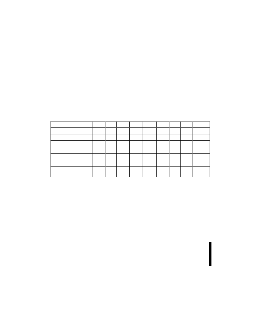
Table 3. Bus Operations for Word-Wide Mode
Mode
Notes
RP#
CE#
OE#
WE#
WP#
A
0
V
PP
DQ
0
–15
Read
1,2,3
V
IH
V
IL
V
IL
V
IH
X
X
X
D
OUT
Output Disable
2
V
IH
V
IL
V
IH
V
IH
X
X
X
High Z
Standby
2
V
IH
V
IH
X
X
X
X
X
High Z
Deep Power-Down
2,9
V
IL
X
X
X
X
X
X
High Z
Intelligent Identifier (Mfr.)
2,4
V
IH
V
IL
V
IL
V
IH
X
V
IL
X
0089 H
Intelligent Identifier (Dvc.)
2,4,5
V
IH
V
IL
V
IL
V
IH
X
V
IH
X
See Table 5
Write
2,6,7,
8
V
IH
V
IL
V
IH
V
IL
X
X
V
PPH
D
IN
NOTES:
1.
2.
3.
4.
5.
6.
7.
8.
9.
Refer to DC Characteristics.
X must be V
IL
, V
IH
for control pins and addresses, V
PPLK
, V
PPH1
or V
PPH2
for V
PP
.
See DC Characteristics for V
PPLK
, V
PPH1
, V
PPH2
voltages.
Manufacturer and device codes may also be accessed via a CUI write sequence, A
1
–A
19
= X
See Table 5 for device IDs.
Refer to Table 6 for valid D
IN
during a write operation.
Command writes for block erase or word program are only executed when V
PP
= V
PPH1
or V
PPH2
.
To program or erase the lockable blocks, hold WP# at V
IH
. See Section 3.3.
RP# must be at GND
±
0.2V to meet the maximum deep power-down current specified.
相關(guān)PDF資料 |
PDF描述 |
|---|---|
| TE28F400B3TA110 | SMART 3 ADVANCED BOOT BLOCK 4-, 8-, 16-, 32-MBIT FLASH MEMORY FAMILY |
| TE28F400B3TA90 | SMART 3 ADVANCED BOOT BLOCK 4-, 8-, 16-, 32-MBIT FLASH MEMORY FAMILY |
| TE28F160B3-T120 | SMART 3 ADVANCED BOOT BLOCK WORD-WIDE |
| TE28F160B3-T150 | SMART 3 ADVANCED BOOT BLOCK WORD-WIDE |
| TE28F400B3-T120 | SMART 3 ADVANCED BOOT BLOCK WORD-WIDE |
相關(guān)代理商/技術(shù)參數(shù) |
參數(shù)描述 |
|---|---|
| TE28F800B5B90 | 制造商:Rochester Electronics LLC 功能描述: |
| TE28F800B5T90 | 制造商:INTEL 制造商全稱:Intel Corporation 功能描述:SMART 5 BOOT BLOCK FLASH MEMORY FAMILY 2, 4, 8 MBIT |
| TE28F800BV-B60 | 制造商:INTEL 制造商全稱:Intel Corporation 功能描述:2-MBIT SmartVoltage BOOT BLOCK FLASH MEMORY FAMILY |
| TE28F800BV-B80 | 制造商:INTEL 制造商全稱:Intel Corporation 功能描述:2-MBIT SmartVoltage BOOT BLOCK FLASH MEMORY FAMILY |
| TE28F800BV-T60 | 制造商:INTEL 制造商全稱:Intel Corporation 功能描述:2-MBIT SmartVoltage BOOT BLOCK FLASH MEMORY FAMILY |
發(fā)布緊急采購,3分鐘左右您將得到回復(fù)。