- 您現(xiàn)在的位置:買賣IC網(wǎng) > PDF目錄383943 > TE28F320B3TC70 (INTEL CORP) 3 Volt Advanced Boot Block Flash Memory PDF資料下載
參數(shù)資料
| 型號(hào): | TE28F320B3TC70 |
| 廠商: | INTEL CORP |
| 元件分類: | DRAM |
| 英文描述: | 3 Volt Advanced Boot Block Flash Memory |
| 中文描述: | 2M X 16 FLASH 2.7V PROM, 70 ns, PDSO48 |
| 封裝: | 12 X 20 MM, TSOP-48 |
| 文件頁數(shù): | 7/58頁 |
| 文件大小: | 920K |
| 代理商: | TE28F320B3TC70 |
第1頁第2頁第3頁第4頁第5頁第6頁當(dāng)前第7頁第8頁第9頁第10頁第11頁第12頁第13頁第14頁第15頁第16頁第17頁第18頁第19頁第20頁第21頁第22頁第23頁第24頁第25頁第26頁第27頁第28頁第29頁第30頁第31頁第32頁第33頁第34頁第35頁第36頁第37頁第38頁第39頁第40頁第41頁第42頁第43頁第44頁第45頁第46頁第47頁第48頁第49頁第50頁第51頁第52頁第53頁第54頁第55頁第56頁第57頁第58頁
28F004/400B3, 28F008/800B3, 28F016/160B3, 28F320B3, 28F640B3
3UHOLPLQDU\
1
1.0
Introduction
This datasheet contains the specifications for the 3 Volt Advanced Boot Block flash memory
family, which is optimized for low power, portable systems. This family of products features
1.65 V–2.5 V or 2.7 V–3.6 V I/Os and a low V
CC
/V
PP
operating range of 2.7 V–3.6 V for read,
program, and erase operations. In addition this family is capable of fast programming at 12 V.
Throughout this document, the term “2.7 V” refers to the full voltage range 2.7 V–3.6 V (except
where noted otherwise) and “V
PP
= 12 V” refers to 12 V ±5%. Section 1.0 and 2.0 provide an
overview of the flash memory family including applications, pinouts and pin descriptions. Section
3.0 describes the memory organization and operation for these products. Sections 4.0 and 5.0
contain the operating specifications. Finally, Sections 6.0 and 7.0 provide ordering and other
reference information.
The 3 Volt Advanced Boot Block flash memory features:
Enhanced blocking for easy segmentation of code and data or additional design flexibility
Program Suspend to Read command
V
CCQ
input of 1.65 V–2.5 V on all I/Os. See Figures 1 through 4 for pinout diagrams and
V
CCQ
location
Maximum program and erase time specification for improved data storage.
NOTES:
1. 32-Mbit and 64-Mbit densities not available in 40-lead TSOP.
2. 4-Mbit density not available in
μ
BGA* CSP.
3. V
CC
Max is 3.3 V on 0.25
μ
m 32-Mbit devices.
4. 4- and 64-Mbit densities not available on 48-Ball VF BGA.
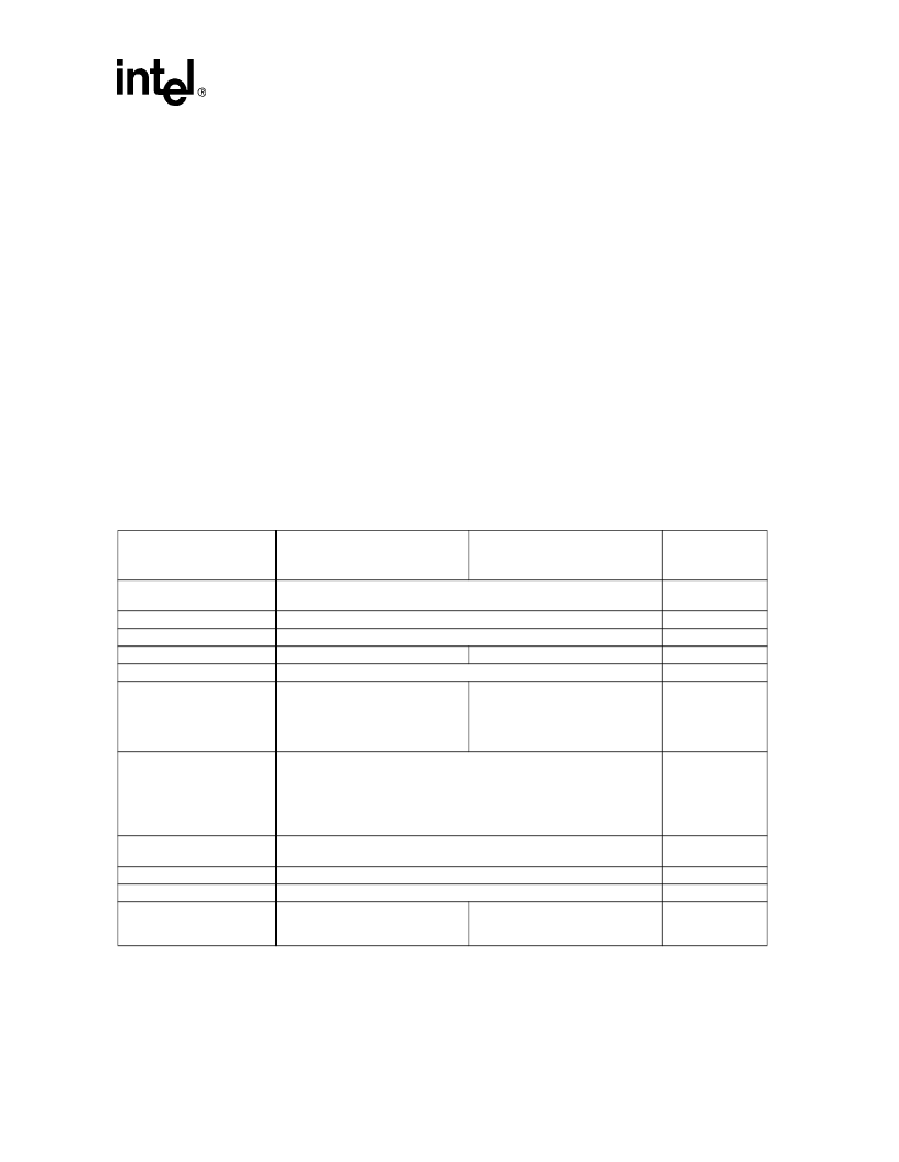
Table 1. 3 Volt Advanced Boot Block Feature Summary
Feature
28F004B3
(2)
, 28F008B3,
28F016B3
28F400B3
(2)
,
28F800B3,
28F160B3, 28F320B3
,
28F640B3
Reference
V
CC
Read Voltage
2.7 V– 3.6 V
Section 4.2
,
Section 4.4
Section 4.2, 4.4
Section 4.2, 4.4
Table 3
Section 4.5
V
CCQ
I/O Voltage
V
PP
Program/Erase Voltage
Bus Width
Speed
1.65 V–2.5 V or 2.7 V– 3.6 V
2.7 V– 3.6 V or 11.4 V– 12.6 V
8 bit
16 bit
70 ns, 80 ns, 90 ns, 100 ns, 110 ns
Memory Arrangement
512 Kbit x 8 (4 Mbit)
1024 Kbit x 8 (8 Mbit),
2048 Kbit x 8 (16 Mbit)
256 Kbit x 16 (4 Mbit),
512 Kbit x 16 (8 Mbit),
1024 Kbit x 16 (16 Mbit),
2048 Kbit x 16 (32 Mbit),
4096 Kbit x 16 (64 Mbit)
Section 2.2
Blocking (top or bottom)
Eight 8-Kbyte parameter blocks
and
Seven 64-Kbyte blocks (4 Mbit) or
Fifteen 64-Kbyte blocks (8 Mbit) or
Thirty-one 64-Kbyte main blocks (16 Mbit)
Sixty-three 64-Kbyte main blocks (32 Mbit)
One hundred twenty-seven 64-Kbyte main blocks (64 Mbit)
WP# locks/unlocks parameter blocks
All other blocks protected using V
PP
Extended: –40
°
C to +85
°
C
100,000 cycles
Section 2.2
Appendix C
Locking
Section 3.3
Table 8
Section 4.2, 4.4
Section 4.2, 4.4
Operating Temperature
Program/Erase Cycling
Packages
40-lead TSOP
(1)
,
48-Ball
μ
BGA* CSP
(2)
48-Lead TSOP,
48-Ball
μ
BGA CSP
(2)
,
48-Ball VF BGA
(4)
Figure 3
,
Figure 4
相關(guān)PDF資料 |
PDF描述 |
|---|---|
| TE28F640B3TC90 | 3 Volt Advanced Boot Block Flash Memory |
| TE28F320B3TC90 | 3 Volt Advanced Boot Block Flash Memory |
| TE28F004SC-100 | BYTE-WIDE SmartVoltage FlashFile MEMORY FAMILY 4, 8, AND 16 MBIT |
| TE28F320B3BA100 | 3 Volt Advanced Boot Block Flash Memory |
| TE28F320B3BC90 | 3 Volt Advanced Boot Block Flash Memory |
相關(guān)代理商/技術(shù)參數(shù) |
參數(shù)描述 |
|---|---|
| TE28F320B3TC90 | 制造商:Intel 功能描述:2M X 16 FLASH 2.7V PROM, 90 ns, PDSO48 |
| TE28F320B3TD70 | 制造商:Rochester Electronics LLC 功能描述:- Bulk 制造商:Intel 功能描述: |
| TE28F320C3 | 制造商:INTEL 制造商全稱:Intel Corporation 功能描述:3 Volt Intel Advanced+ Boot Block Flash Memory |
| TE28F320C3B110 | 制造商:INTEL 制造商全稱:Intel Corporation 功能描述:3 VOLT ADVANCED+ BOOT BLOCK 8-, 16-, 32-MBIT FLASH MEMORY FAMILY |
| TE28F320C3B90 | 制造商:INTEL 制造商全稱:Intel Corporation 功能描述:3 VOLT ADVANCED+ BOOT BLOCK 8-, 16-, 32-MBIT FLASH MEMORY FAMILY |
發(fā)布緊急采購,3分鐘左右您將得到回復(fù)。